


News: Microelectronics
23 August 2024
High-current vertical diamond MOSFETs
Waseda University in Japan reports on vertical metal-oxide-semiconductor field-effect transistors (MOSFETs) constructed from diamond with up to 0.7A maximum drain current [Nobutaka Oi et al, IEEE Electron Device Letters, published online 7 August 2024]. The team claims the 0.7A drain current as the largest reported so far for diamond FETs. Two of the five researchers involved are also affiliated with Japan-based Power Diamond Systems Inc.
Diamond FET devices are potentially a p-type complement for the n-channel devices that are fabricated in silicon carbide (SiC), gallium nitride (GaN) and gallium oxide (Ga2O3) material systems that are being developed for power electronics applications. Complementary MOSFETs would enable the use of CMOS circuit designs, which enable higher-speed operation and smaller gate drive requirements. In the power domain, efficient complementary inverters are wanted for DC/AC conversion of renewable and stored energy sources.
Diamond material properties suitable for power applications include a high breakdown field (10MV/cm), high thermal conductivity (22W/cm-K), and high hole mobility (2000–3800cm2/V-s).
Two epitaxial diamond layers, 0.5μm undoped and 1.0μm n-type, were added to a 3mmx3mmx0.3mm p+-type boron-doped diamond substrate (Figure 1) by microwave plasma chemical vapor deposition (MPCVD). The carbon came from a mix of methane (CH4) and carbon dioxide (CO2). The n-type nitrogen doping was sourced from nitrogen gas (N2).
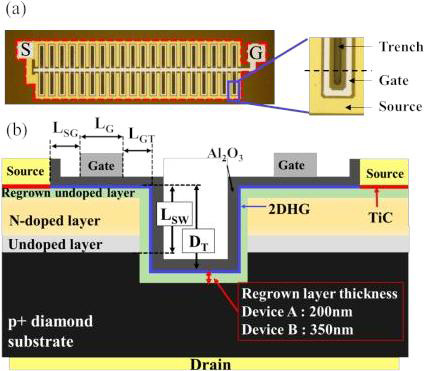 Figure 1: (a) Optical microscope image and close-up of device with gate width of 5mm (S: source, G: gate) (b) Cross-sectional schematic of dash line area.
The vertical FET structure was fabricated by inductively coupled plasma reactive-ion etch (ICP-RIE), MPCVD diamond regrowth, electron-beam evaporation of the source electrode, plasma treatments for hydrogen termination and device isolation, 450°C atomic layer deposition (ALD) of 200nm aluminium oxide (Al2O3), tetramethylammonium hydroxide (TMAH) Al2O3 etch, dual ion beam sputtering of the back-side drain contact, and thermal evaporation of the gate and source contact pad.
The ICP-RIE to a depth of 2.2μm created 60μm-wide trenches. The trench length was 5μm. The vertical channel consisted of a two-dimensional hole gas (2DHG) that formed near the interface between the regrown diamond and Al2O3 layers.
The source electrode consisted of titanium/platinum/gold (Ti/Pt/Au), annealed to form titanium carbide (TiC) as the diamond source contact. The drain was Ti/Au. The gate and source pad were Al.
The gate length (LG) was 4μm. The gate widths, the perimeters of the trenches, were varied on a millimeter scale. The distances of the gate from the source (LSG) and trench (LGT) were 2μm and 3μm, respectively.
A device with 10mm gate width achieved a maximum drain current of −0.7A at −20V drain bias, and −20V gate potential. The regrown layer thickness was 200nm (i.e. device type ‘A’).
The on/off current ratio was around 9.5 orders of magnitude with the off-current reaching down to the measurement limit of the team’s equipment (~10−11A) when the gate was at 35V.
With a −1V drain bias, the threshold voltage was +21.2V, so the device operated in a normally-on (when the gate potential is 0V) depletion mode. For many power applications, a normally-off mode is preferred.
Another device A, with 0.1mm gate width, achieved an off-state (+30V VGS) breakdown voltage of 225V. The drain current was less than 10−10A almost up to the breakdown point.
The team comments: “Breakdown voltage is expected to be lower for devices of larger gate width because of inhomogeneous distribution of device characteristics due to process non-uniformity.”
The drain current density normalized by the gate width tended to fall for the wider devices (Figure 2). Also, a thicker 350nm (‘B’) regrown layer gave around 30% higher drain current for the 1mm-wide FETs tested.
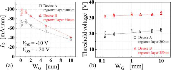
Figure 2: (a) Drain current density (ID) versus gate width (WG) at −10V VDS and −20V VGS. (b) Threshold voltage dependence on gate width.
The researchers comment: “The tendency for the drain current density to decrease as WG increases suggests the presence of additional resistances such as substrate resistance and source electrode resistance, with the latter expected to play a more significant role.”
For devices wider than 2mm, the measurements were made in pulse mode to avoid self-heating effects.
The threshold voltages were larger for the B series, meaning that they were deeper into depletion-mode territory. The specific on-resistances were 48.4m Ω-cm2 and 36.7m Ω-cm2 for 2mm WG devices A and B, respectively. These values were reduced by subtracting the effect of the source electrode area from the total active area to 17.7m Ω-cm2 and 13.8m Ω-cm2, respectively. The team suggests that the electrode contact resistance could be improved through use of an interlayer dielectric and reduction of device dimensions.
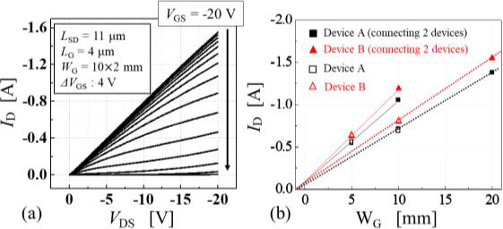
Figure 3: (a) ID-VDS pulse mode characteristics of two connected B devices with VGS ranging from −20V to +36V. (b) Relationship between drain currents of single and double devices at −20V VDS and −20V VGS.
To achieve more than 1A drain current, the researchers connected two devices (Figure 3). For 10mm wide device B, two devices enabled −1.5A to be reached with an on-resistance of 12.7 Ω, just over half the value for a single FET. The maximum drain current for type A was −1.3A.
The author Mike Cooke is a freelance technology journalist who has worked in the semiconductor and advanced technology sectors since 1997.


