News: Microelectronics
19 December 2024
Fully vertical GaN p-i-n diodes on silicon
Researchers from France’s Institute of Electronics, Microelectronics and Nanotechnology (IEMN) and Siltronic AG in Germany claim the first demonstration of high-current operation (above 10A) for vertical gallium nitride (GaN)-based devices on silicon (Si) substrates [Youssef Hamdaoui et al, IEEE Transactions on Electron Devices, published online 20 November 2024].
The team comments: “The diodes deliver an unprecedented high ON-state current with more than 11.5A for a 1mm anode diameter. This is ascribed to both the optimization of backside N-face ohmic contacts and the implementation of thick copper electroplating replacing the silicon substrate as a heat sink.”
The devices used a fully vertical, rather than pseudo-vertical, structure. ‘Pseudo-vertical’ refers to a device where all the contacts are made on the front-side of the chip or wafer. While the current flow in the main body of the device is approximately vertical in such arrangements, the current flows laterally in the n-contact layer. The result is that current-crowding effects tend to reduce the power-handling capability of pseudo-vertical devices.
The fully vertical structure promises higher breakdown voltages, along with reduced on-resistance delivering higher currents. Production on silicon substrate, rather than silicon carbide or bulk/freestanding GaN, should also make GaN devices more competitive for low-cost applications.

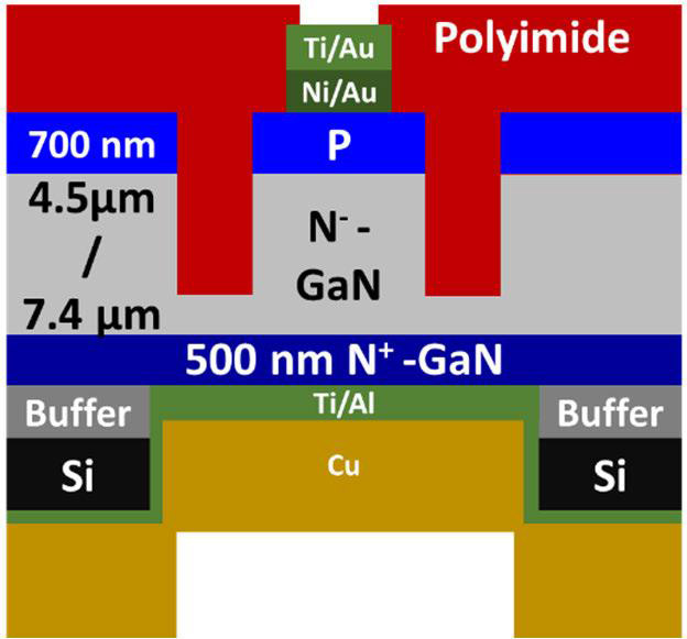
Figure 1: (a) Schematic cross section of fully vertical p-i-n diode. (b) Focused ion beam cross-section image. (c) Optical image of wafer backside after silicon and buffer removal where the front-side circular diodes appear by transparency.
Two six-inch GaN/Si wafers were prepared (Figure 1) by metal-organic chemical vapor deposition (MOCVD). One wafer had a 4.5μm lightly n-doped (n−) drift layer. The other wafer had instead a 7.4μ drift region. The silicon doping concentration in the drift layers was 3x10¹⁶/cm3 with 9x10¹⁵/cm3 net ionized electron density, according to electrochemical capacitance–voltage (ECV) measurements. The thicker drift layer should be able to withstand higher voltages, but at the cost of higher on-resistance.
Inspection with a transmission electron microscope (TEM) in weak beam darkfield mode determined a threading dislocation density of order 5x10⁸/cm2. Hall-effect measurements gave a mobility value for the drift layer at 756cm2/V-s.
The p-i-n diodes were fabricated, beginning with the deep beveled mesa used as edge termination. The deep etching was carried out by plasma reactive ion etch (RIE), and the bevel by inductively coupled plasma (ICP) etch. The purpose of the edge termination was to spread the electric field at the junction periphery, and to reduce leakage.
The anode contact to the p-GaN layer was through an annealed nickel/gold (Ni/Au) ohmic electrode, followed by a titanium/gold (Ti/Au) contact pad.
The front-side of the device was passivated with polyimide, which also filled the deep mesa trenches to provide enhanced mechanical strength to the membrane structures of the final devices. The polyimide was applied in a three-stage spin-coat process. The initial spin speed was slow to ensure filling of the trenches, particularly in the corners. The spin-speed was increased to improve coating uniformity, and then further increased to increase the coat thickness.
The front-side was completed with a silicon dioxide (SiO2) protection layer.
The silicon substrate was thinned from 1mm to 300μm by back-side thinning. Local etching under the p-i-n diodes was achieved by deep RIE to remove the intervening silicon, followed by ICP etch of the GaN buffer layer to access the n-GaN contact layer. The circular membrane regions were 3mm diameter. The etched membrane surface was treated with hydrochloric (HCl) acid to reduce the n-contact resistance from more than 10−4Ω-cm2 without treatment to 9x10⁻⁶Ω-cm2 after treatment.
The backside was completed with deposition of the titanium/aluminium (Ti/Al) cathode ohmic contact, and electroplating of 300μm copper (Cu) as a heat-sink.
The team comments: “It is important to note that the highly strained thick Cu deposition is enabled by the polyimide protection on the front-side that strengthens the mechanical robustness of the membranes, otherwise resulting in cracked and damaged devices.”
The reverse-bias breakdown voltage of diodes with 7.4μm drift layer reached 1230V. The researchers estimate a critical electrical field at the junction of more than 2.2MV/cm, and 1.66MV/cm average across the drift layer.
The breakdown was soft/recoverable. The researchers see this as hinting at an avalanche mechanism, which is “an essential feature for the industrialization of these new types of devices”.
The team comments: “Avalanche breakdown provides a safe leakage current path that protects the devices from irreversible damage. In this case, the leakage current is induced by the impact ionization of the accumulated carriers when exceeding a specific energy. Increasing the temperature causes a delay in the onset of impact ionization due to phonon scattering.”
The breakdown voltage (BV) on small diodes, less than 100μm diameter, increased slightly with temperature, presumably due to the increased number of phonons delaying impact ionization. For larger devices, soft breakdown was observed, and the voltage did not increase with temperature, leading to hard breakdown effects.
The researchers explain: “The absence of soft breakdown for large diodes is attributed to the larger amount of defects that may contribute to increase the leakage current, especially at high temperature preventing the avalanche phenomenon. This suggests that defect-assisted tunneling or trap-assisted recombination may dominate the leakage current in these devices.”

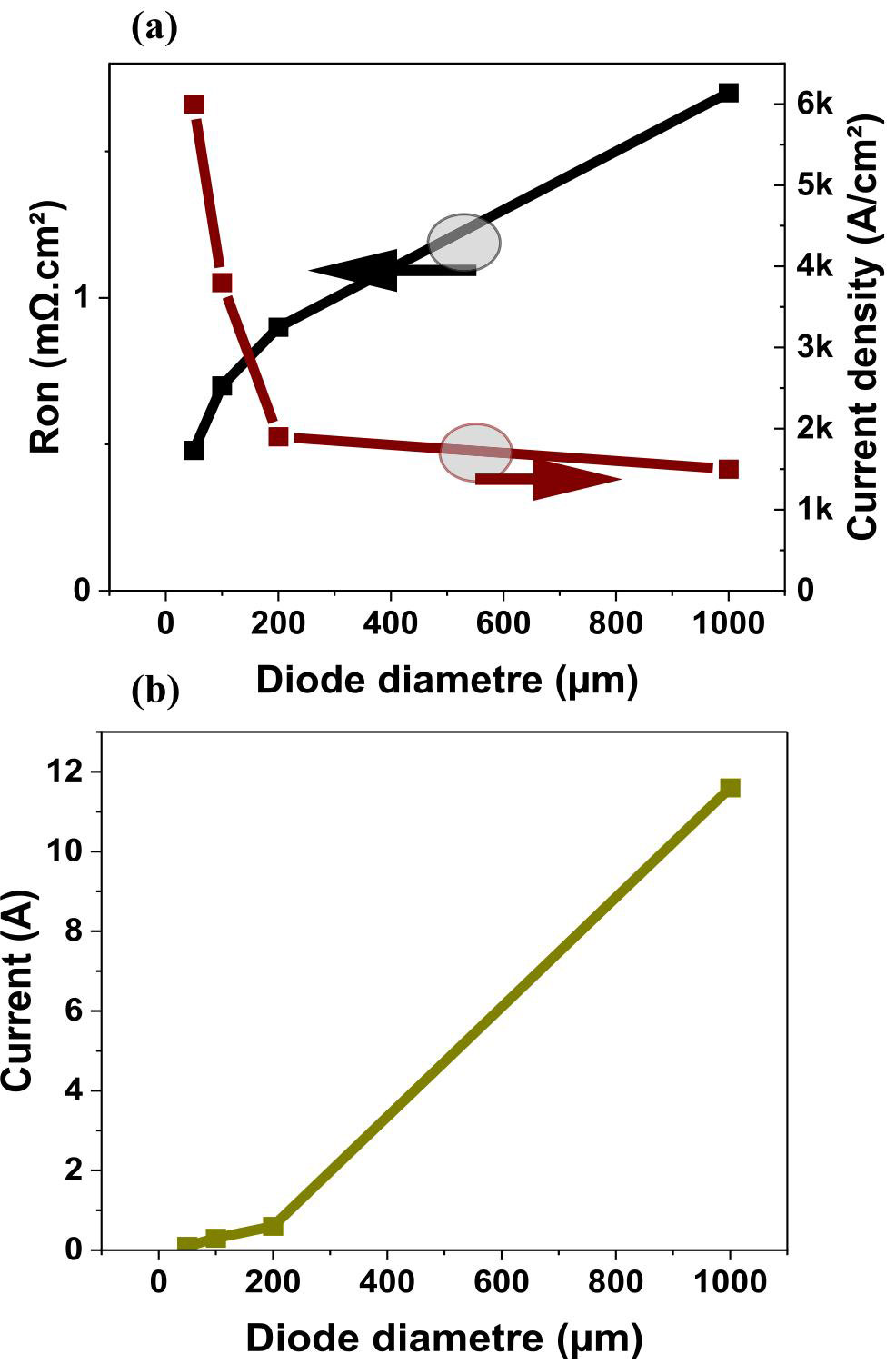
Figure 2: (a) Extracted Ron,sp and on-state current density. (b) Forward current versus diode anode diameter at 8.5V.
The turn-on voltage of the small and large devices was around +5V. The current at 8.5V roughly scaled with device size from 100mA to 11.6A (Figure 2). The larger diodes, more than 200μm diameter, were operated in pulse mode to avoid self-heating effects. The smaller devices were tested in continuous wave (CW) mode. The specific on-resistance (Ron,sp) of small diodes with 50μm-diameter anode was 0.48mΩ-cm2. For 1mm diameter, Ron,sp was 1.7mΩ-cm2.
The optimization of the copper heat-sink layer and packaging could further improve the thermal management over pulse operation, reducing Ron,sp in the larger diodes, the team believes.

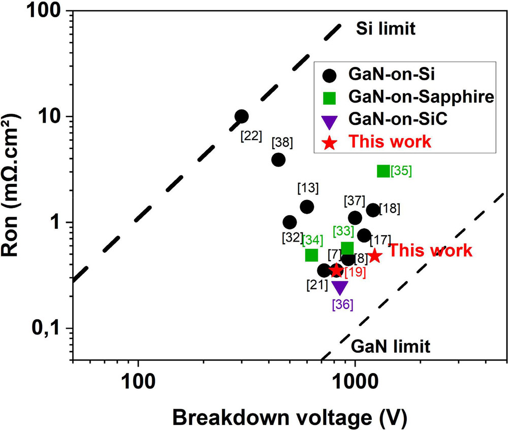
Figure 3: Benchmark of fully and pseudo-vertical small GaN-on-foreign substrate diodes.
The small diodes achieved Baliga figures of merit (BFOMs) up to 3.17GW/cm2 (BV2/Ron,sp), representing the balance between BV and Ron,sp (Figure 3).
The author Mike Cooke is a freelance technology journalist who has worked in the semiconductor and advanced technology sectors since 1997.


