News: LEDs
13 December 2024
Red InGaN LEDs on scandium aluminium magnesium
Researchers at Saudi Arabia’s King Abdullah University of Science and Technology (KAUST) and Japan’s Aichi Institute of Technology claim the first demonstration of fully indium gallium nitride (InGaN) red light-emitting diodes (LEDs) on a scandium aluminium magnesium, ScAlMgO4 (SAM), substrate [Mohammed A. Najmi et al Appl. Phys. Express, v17, p111001, 2024].
The researchers comment: “The material quality is currently far from that of state-of-the-art red LEDs grown on GaN/sapphire and GaN/Si, and therefore the device performance shows a significant disparity. However, the InGaN/SAM configuration has the potential to improve the material quality due to the lattice matching. Improvement of the material quality, and the interface between the InGaN and SAM substrates, could significantly enhance the efficiency of the red LEDs.”
The lattice-matched composition to SAM is In0.17Ga0.83N. Red InGaN LEDs are being developed in particular for combination with green and blue InGaN devices in full-color display deployments. The advantage would be simpler processing compared with mixing devices from other III–V compound semiconductor families, such as indium gallium arsenide phosphide (InGaAsP).
The team explains: “The requirements of display systems necessitate integrating these three primary colors of light emitters into one pixel. RGB emitters can all be realized through alloying III–nitrides (GaN, InN) due to their bandgap versatility. This advantageous characteristic makes III–nitrides particularly suitable for display applications. Despite the theoretical possibility of color tunability, achieving efficient InGaN-based longer-wavelength LEDs/LDs remains an unresolved research problem within the III–nitrides community.”
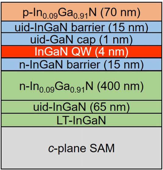
The LED’s epitaxial structure was grown by metal-organic vapor phase epitaxy (MOVPE) on c-plane SAM substrate (Figure 1). The buffer layer, designed to give a Ga-polar structure, was grown at low temperature (LT). The team reports that a Ga-polar structure reduces residual electron concentrations, “and enables us to realize an effective p-type InGaN layer.”

Figure 1: Schematic view of LED structure.
Hall measurements on the sample gave a p-type conductivity with an effective 8x10¹⁷/cm3 hole concentration and 0.7cm2/V-s mobility. The resistivity was 11Ω-cm.
The researchers comment: “The (0002) and (10–12) x-ray rocking curve values of the Si-doped In0.09Ga0.91N layer were 1354arcsec and 2452arcsec, respectively.” Although molecular beam epitaxy can achieve narrower x-ray peaks for InGaN/SAM, MOVPE typically renders material with 2500–3000arcsec full-widths at half maximum (FWHMs) for the (0002) peak. The team has previously achieved N-polar InGaN/SAM material with 940arcsec and 1960arcsec FWHMs, respectively, for the (0002) and (10-12) peaks. Unfortunately, this material had a high ~1019 electron concentration and a rough surface.
The researchers found a high V-pit density, suggesting a high threading dislocation density. The team comments: “The high density of dislocations can be attributed to the presence of the LT-buffer layers. The underlying layers consist of a Si-doped n-InGaN layer with an LT-buffer InGaN. The material quality of the LT-buffer layers is expected to be inferior to the directly grown InGaN on SAM due to the amorphous phase resulting from LT growth.”
Also, the researchers suggest that the relatively low growth temperature of the device layers (825°C) was not sufficient to recrystallize the material grown on top of the LT buffer layer. High-quality GaN is generally grown at temperatures around 1000°C.
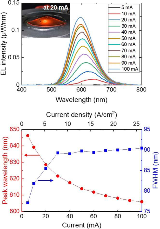
Electroluminescence (EL) spectra showed wide single peaks (Figure 2). At 20mA the peak position was at 629nm, just in the red range of the visible spectrum (625–750nm). At the lower 5mA injection, the peak was more established in the red range at 647nm, but at higher currents the peak shifted out of the red region (617nm at 40mA) into to shorter orange wavelengths (590–625nm), towards the blue end of the the visible spectrum.

Figure 2: (a) Red LED electroluminescence (EL) spectra with different current injections at room temperature. Inset: photograph of EL at 20mA. (b) Peak wavelengths and FWHMs versus current injections.
“This blue-shift behavior is a typical phenomenon of c-plane InGaN-based LEDs caused by the quantum confined Stark effect (QCSE),” the team explains. The QCSE arises from the strain-generated electric fields in the epitaxial structure and the different charge polarization behaviors of the partial ionic III–N chemical bonds.
The team also suggests that the compositional fluctuations of InGaN in the quantum well structure could lead to shorter-wavelength regions being more active as the current injection increases, and the higher turn-on voltage bias is reached, adding to the blue-shift effect. The fluctuations also contribute to widening the peak at higher injection.
The researchers also blame the SAM substrate quality for the non-ideal EL emission behavior. In particular, the substrates have step/terrace structures, affecting the subsequent epitaxial growth quality.
The researchers comment: “The prospect of LEDs with narrow FWHMs and small blue-shifts can potentially be achieved using a cleaved substrate, which allows for the fabrication of a completely step-free surface. Alternatively, we suggest that a large misoriented substrate with a highly dense step and terrace structure may also be acceptable for achieving uniform InGaN layer growth.”

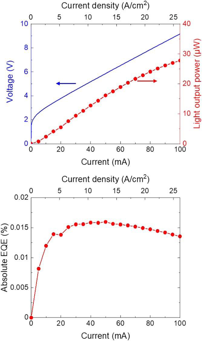
Figure 3: (a) Forward voltage and light output power (b) absolute EQE values at different injection currents.
The external quantum efficiency (EQE) reached 0.016% at 40mA injection and 12.6μW light output power (Figure 3). At 20mA the light output and EQE were 5.5μW and 0.014%, respectively.
Red LEDs InGaN GaN Scandium aluminium magnesium MOVPE
https://doi.org/10.35848/1882-0786/ad8f0e
The author Mike Cooke is a freelance technology journalist who has worked in the semiconductor and advanced technology sectors since 1997.


