News: Optoelectronics
27 December 2024
Near-room temperature 8μm interband cascade lasers
Researchers based in China and the USA report the highest operation temperatures so far for interband cascade lasers (ICLs) emitting at wavelengths around 8μm [Yuzhe Lin et al, Optics Express, v32, p46439, 2024].
The team, from the Institute of Semiconductors and Nanjing University in China and University of Oklahoma in the USA, sees advantages of ICLs over quantum cascade lasers (QCLs) for many applications.
“The output powers of ICLs are lower with smaller currents and reduced voltages than what can be achieved in QCLs. However, several milliwatts of output power are sufficient for many sensing applications and lower power consumption is a more important figure of merit. Hence, in such scenarios, ICLs with a low threshold current and reduced voltage would be more desirable.”
The reported devices continued operating in pulse mode up to around 280K, around 20 degrees short of typical room temperatures of around 300K (27°C), and more than 50K higher than previous reports.
The researchers comment: “Considering that the attained operating temperature is already close to RT, with additional effort in optimizing design parameters, RT operation of ICLs should be achievable in the wavelength region near 8μm.”

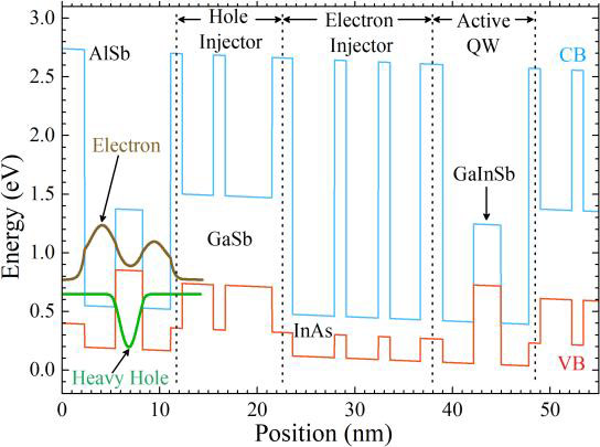
Figure 1: Schematic band diagram of one cascade stage and layer sequence under an applied electric field of 70kV/cm.
The ICL structures were grown by molecular beam epitaxy on n-type indium arsenide (InAs) wafers with 18 gain stages (Figure 1). Two wafers were prepared, F and G, with slightly different layer thicknesses. Wafer F had layers with aluminium antimonide (AlSb)/InAs/gallium indium antimonide (Ga0.65In0.35Sb)/InAs/AlSb in a thickness sequence 23/31.5/28/28.5/12Å. In wafer G the InAs/GaInSb/InAs section was changed in thickness to 32.5/26/29.5Å, aiming at a longer emission wavelength.
The gain stages were placed within a waveguide structure consisting on each side of inner 0.73μm InAs separated-confinement layers (SCLs), intermediate 1.5μm InAs/AlSb superlattices (Sls), and n+-InAs outer cladding. The SL cladding was also doped at two levels with a view to reducing losses associated with free-carrier absorption (FCA). Such a hybrid cladding waveguide structure has been widely used to enhanced the performance of ICLs over a range of wavelengths.
The materials were fabricated into 2mm-long broad-area lasers of 100μm and 150μm widths, using wet etching. The devices were mounted on copper heatsinks epi-side up, fastened with indium solder.
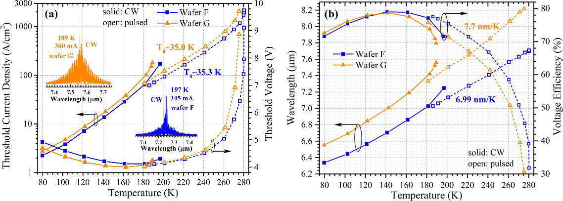
One 100μmx2mm device from wafer F continued lasing up to 280.4K with a 7.7μm emission wavelength (Figure 2). The lasing threshold current density was 2150A/cm2. The current was pulsed at 5kHz with 500ns duration (the pulse width was increased to 1μs for temperatures below 270K). A similar device from wafer G lased up to 275.5K with 2070A/cm2 threshold. The wavelength was 8.22μm.

Figure 2: (a) Threshold current density and threshold voltage versus temperature, and insets continuous wave (CW) emission spectra; and (b) lasing wavelength and voltage efficiency versus temperature for 100μm-wide F/G devices.
At 80K, the wafer F device achieved a 2.25A/cm2 threshold, and the wavelength was 6.34μm. The G device threshold was 2.75A/cm2 with 6.55μm emission wavelength.
The researchers comment: “Such low threshold current densities at 80K imply very high quality of the grown materials with notable low Shockley–Read–Hall recombination.” The maximum voltage efficiency reached 79% at 140K (CW) in both devices, “the highest among semiconductor lasers at these long wavelengths,” the team adds.
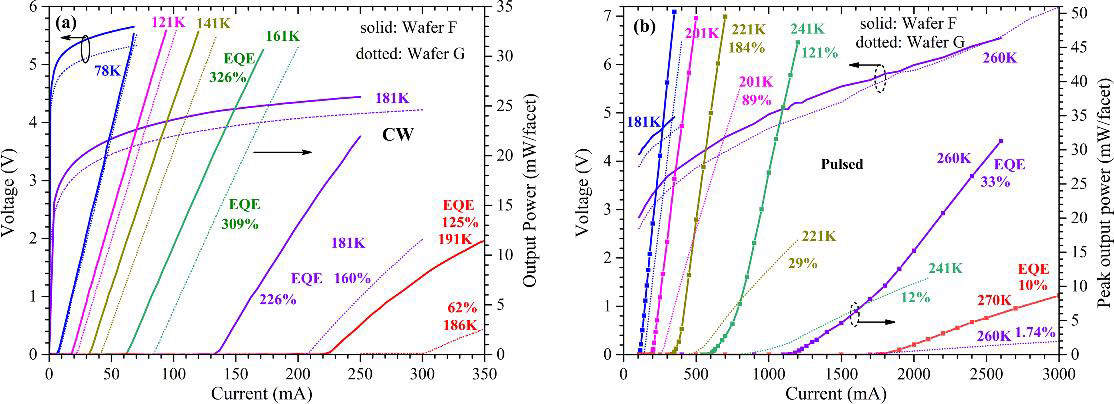
The slope efficiency at 78K was 500mW/A/facet (Figure 3), which gives an external quantum efficiency (EQE) of more than 500%. In ICLs, each electron flowing through the device can emit multiple photons, allowing EQEs above 100%.

Figure 3: (a) CW and (b) pulsed current-voltage–light output power characteristics of 100μm-wide devices from wafers F and G at various temperatures.
The researchers also used simulations as a guide towards potential enhancements in future work. A particular concern was FCA and plasmonic effects. The FCA loss could be reduced with lower doping levels.
The team is also concerned that there could be “substantial absorption loss due to intervalence-subband-transitions”. Researchers based in Austria and Germany have shown that this effect can be ameliorated with valence-band engineering, which the team also plans to explore.
Interband cascade lasers AlSb InAs GaInSb
https://doi.org/10.1364/OE.546307
The author Mike Cooke is a freelance technology journalist who has worked in the semiconductor and advanced technology sectors since 1997.


