News: LEDs
5 December 2024
Graded barriers bandwidth boost for micro-LEDs on silicon
South China University of Technology and Guangdong Choicore Optoelectronics Company Ltd in China report on using graded indium gallium nitride (InGaN) quantum barriers (QBs) in blue light-emitting diode (LED) to improve the modulation frequency performance of devices grown on silicon (Si) with a view to deployment in visible light communication (VLC) systems [Lei Lei et al, IEEE Electron Device Letters, published online 11 November 2024].
The team sees VLC as a potential supplement to the overcrowded spectrum of existing wireless communication systems. “However, the lack of LED performance severely limits the development of VLC,” the researchers point out.
VLC could be used in systems aimed at short-range positioning data exchange, indoor internet, etc. Such systems can be integrated into existing lighting infrastructure. Normal-size LEDs tend to have relatively low modulation bandwidths in the tens of MHz range. This can be improved by reducing the size of the LEDs. One drawback is that the smaller devices have lower light output power (LOP), impacting the signal to noise ratio.
One of the blockages to improving the frequency performance of InGaN LEDs is the built-in electric fields that arise from charge polarization contrasts of the III-nitride device layers. These fields tend to reduce the radiative efficiency due to the field pulling apart the electrons and holes that need to combine to emit photons.
By grading the InGaN barriers the researchers hoped to screen these fields, improving both bandwidth and LOP performance.

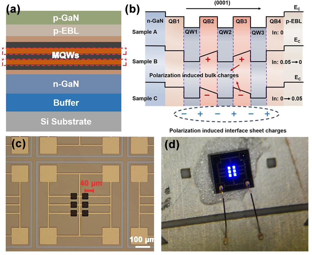
Figure 1: Schematic diagrams: (a) Si-substrate GaN-based LED epitaxial structure, and (b) conduction band for three samples. (c) Optical microscope image of sample, and (d) image of sample C operating at 10A/cm2.
The epitaxial structures used included 3μm n-GaN contact, 3x(3nm/4nm) In0.16Ga0.84N/InxGa1−xN multiple quantum well (MQW), 30nm p-type aluminium gallium nitride electron-blocking layer (EBL), and 60nm p-GaN contact layers (Figure 1). Three samples were processed with different InxGa1−xN profiles in the QBs: sample A had conventional pure GaN in the QBs 1–4 (i.e. x=0); sample B had the middle two QBs, 2 and 3, linearly graded from 5% to 0% along the (0001) growth direction, with the outer barriers pure GaN; and, sample C had the QBs graded in the opposite sense, from 0% to 5%.
According to simulations, the effect of the grading in sample C was to elevate the height of the triangular deep potential well between the last QB and the EBL, while diminishing the height of the valence-band barrier.
The team comments: “Such alterations are conducive to enhancing hole injection efficiency and mitigating electron escape, achieving a simultaneous increase in bandwidth and LOP of samples.”
The epitaxial material was fabricated into 2x3 arrays of micro-LEDs flipped onto a silicon conductive circuit substrate and bonded with gold/tin (Au/Sn). The micro-LEDs included a silver (Ag) reflector on the p-contact layer. The individual micro-LED units measured 40μmx40μm. The n-GaN contact layer was wired in parallel with sputtered titanium/aluminium/platinum/gold (Ti/Al/Pt/Au).
The devices needed slightly different forwardvoltage biases to give 1000A/cm2 current injection: 3.46V for sample A, and 3.44 and 3.41V for B and C, respectively.
The team comments: “Sample A has the highest voltage, potentially because of the higher series resistance and lower crystal quality. Moreover, the weaker polarization field in sample C decreases the height of triangle barrier of the valence band that the carriers need to overcome to inject into the MQWs, and thus the forward voltage.”
Sample C also showed 11% improvement over A in terms of light output power (LOP) — 28.9mW, compared with 26.1mW at 2000A/cm2. Array B had a LOP of 26.7mW at the same current injection point.
The peak wavelength shifted to shorter wavelengths in moving from low to medium current injection: 22nm in sample A, 19.1nm for B, and 17.9nm for C. The peak wavelength at the lowest current was around 450nm (~5nm higher for A, and ~5nm lower for C) The smaller shifts in B and C was attributed to the InGaN grading, and for C the favorable charge polarization configuration in the barriers. The external quantum efficiency for sample C was also improved by 10% over that of sample A (~5%) at 2000A/cm2.

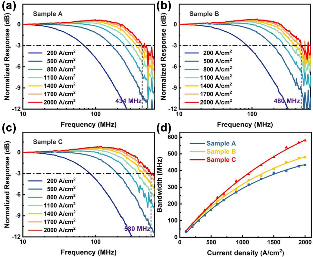
Figure 2: (a)-(c) Frequency responses of samples A–C under different current densities. (d) −3dB bandwidth versus current density.
Sample C also demonstrated a higher −3dB bandwidth — 580MHz at 2000A/cm2, compared with 434MHz and 480MHz for samples A and B, respectively (Figure 2).
The researchers comment: “The enhancement in −3dB bandwidth could be due to the weaker polarized electric field, which favors accelerated carrier radiative recombination. Concurrently, the lowered triangle barrier of the valence band causes an increase in hole concentration within the active region, thereby further enhancing the radiative recombination coefficient B.”

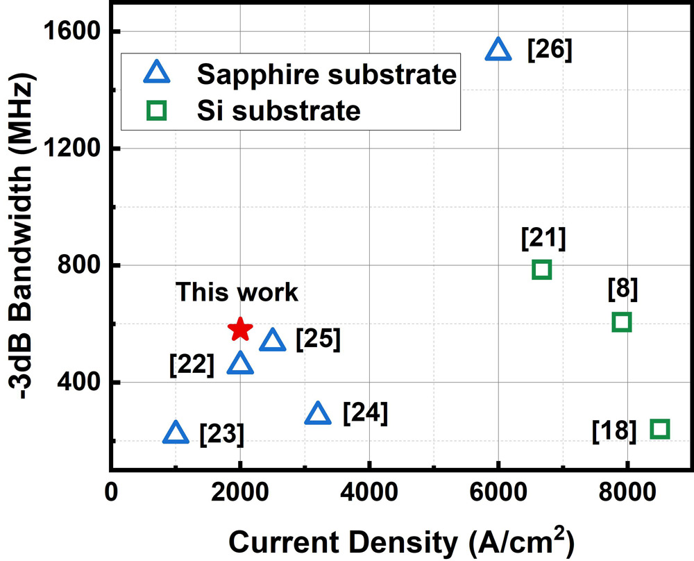
Figure 3: Comparison of −3dB bandwidth for micro-LED arrays with previous reports.
Comparing the bandwidth with previous research shows the South China/Guangdong sample C devices to have performance comparable to those grown on sapphire: high bandwidth at lower injection current density, compared with reports of LEDs on silicon.
Micro-LEDs on silicon InGaN GaN
https://doi.org/10.1109/LED.2024.3495654
The author Mike Cooke is a freelance technology journalist who has worked in the semiconductor and advanced technology sectors since 1997.


