


News: Microelectronics
9 February 2024
Fully vertical GaN-on-SiC Schottky barrier diodes with low on-resistance
Beijing University of Technology and Peking University in China have reported improved performance for fully vertical Schottky barrier diodes (SBD) fabricated from gallium nitride on silicon carbide substrate (GaN/SiC) by using an ultrathin aluminium gallium nitride (AlGaN) buffer instead of the more usual complex, thick AlN/AlGaN structures [Yuting Sun et al, Semicond. Sci. Technol., published online 24 January 2024].
The team comments: “This epitaxial strategy can also be used for SiC/GaN heterogeneous integration by combining the merits of both GaN and SiC on a single platform.”
The researchers further implemented other enhancements such as employing cap layers to protect against material decomposition during high-temperature annealing, and fluorine ion implants for edge termination.
Vertical GaN electronics structures enhance the ability to handle high power and voltage since the peak electric field usually occurs far from the surface, enhancing robustness against breakdown, unlike in lateral devices. The best performing vertical devices are produced on freestanding or bulk GaN substrates, but these tend to be small and costly.
Recent developments in SiC substrate manufacturing have resulted in 8-inch diameter wafers becoming commercially available from Wolfspeed and Tankeblue for mass production, raising the prospect for lower costs for SiC and GaN/SiC devices. A further advantage of SiC as a base for GaN power electronics is SiC’s high thermal conductivity, enabling better thermal management of Joule heating effects.
The III–nitride layers for the vertical SBD (Figure 1) were grown on n+-SiC substrate, using metal-organic chemical vapor deposition (MOCVD). The substrate was pre-treated with trimethyl-aluminium before MOCVD of a 700nm n+-GaN buffer layer.
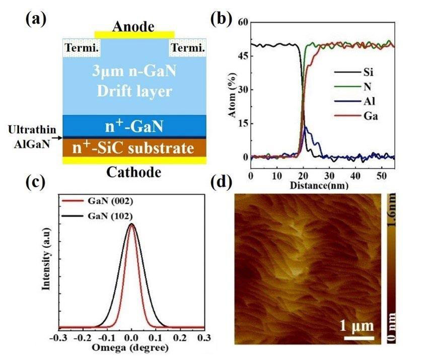
Figure 1: (a) Schematic cross-section of fully vertical GaN-on-SiC SBD. (b) EELS profiles obtained at GaN/SiC interface. (c) Symmetric (002) and asymmetric (102) x-ray diffraction rocking curves and (d) AFM image (5 μmx5 μm) of GaN grown with ultrathin AlGaN buffer.
The pre-treatment resulted in an ultra-thin layer of AlGaN forming through inter-atomic self-diffusion at the GaN/SiC interface. The AlGaN layer was measured at 2nm thick, according to electron energy-loss spectroscopy (EELS).
The III-nitride epitaxy was completed with a 3 μm n−-GaN drift layer. The root-mean-square roughness was 0.22nm, according to atomic force microscopy (AFM).
The researchers comment: “The reasonable crystal quality and surface roughness demonstrate the effectiveness of the ultrathin AlGaN buffer layer on accommodating the mismatch between GaN and SiC.”
The ohmic cathode contact consisted of annealed nickel. The researchers used a silicon dioxide (SiO2) capping layer to retain material quality during the 900 C rapid thermal annealing (RTA) process. The cap was removed by a hydrofluoric acid dip. Without the cap layer the AFM surface roughness increased significantly, with the GaN atomic surface steps completely disappearing. By contrast, the AFM roughness of the capped device material only increased slightly.
The surface decomposition of non-capped annealing results in reduced Schottky metal/semiconductor contact quality and thus deterioration of the current–voltage behavior.
The researchers report: “Although the surface roughness increased from 0.22nm to 0.28nm with a little more surface pits after annealing, orderly arranged atomic steps were still clearly visible on the GaN surface of the improved SBD. These results indicate that the SiO2 capping layer can effectively protect the GaN surface against decomposition during RTA.”
The device was completed with fluorine ion implantation for edge termination, and deposition of nickel/gold for the Schottky anode contact.
The use of an ultrathin AlGaN layer reduced the specific on-resistance (RON,sp) of the SBD to 1.5m -cm2, compared with 50m -cm2 for a reference SBD with 50nm-thick heavily doped Al0.25Ga0.75N buffer layer. The researchers attribute the better performance of the ultrathin AlGaN layer SBD to increased tunneling current, while the much larger band offset of the thick AlGaN buffer weakens the tunneling capability.
In terms of device performance, capping during RTA reduced on-resistance by a factor of almost 2. The Schottky barrier height was 0.79eV with capping, and 1.02eV without. Also, capping during RTA reduced the ideality factor from 1.22 to 1.08 (ideal=1). Further, the corresponding on/off current ratios were 8.5x10⁶ and 5x10⁹, an improvement of almost three orders of magnitude (28dB).
The improved SBD with capping during RTA had an on-resistance of 0.85m -cm2, which the team describes as “a relatively small value among the reported vertical GaN diodes on foreign substrates fabricated by complex fabrication process”.
The forward current at 3V bias reached 1.8kA/cm2 density. The team comments: “The superiority of the forward I–V characteristics indicate that the ultrathin AlGaN buffer layer is effective for realizing fully vertical GaN SBD on SiC substrate with low RON,sp and stable conductivity based on simplified epitaxy stack.”
The effect of increasing the device temperature in the range 25–120 C was found to be a slow ramp in RON,sp of 0.00345m -cm2/ C. The turn-on voltage was simultaneously affected by a slow decrease rate of 0.0016V/ C.
The researchers found the effect of the fluorine ion termination (FIT) to be an increase in reverse breakdown voltage (BV, for 1A/cm2) from 108V to 214V (Figure 2).
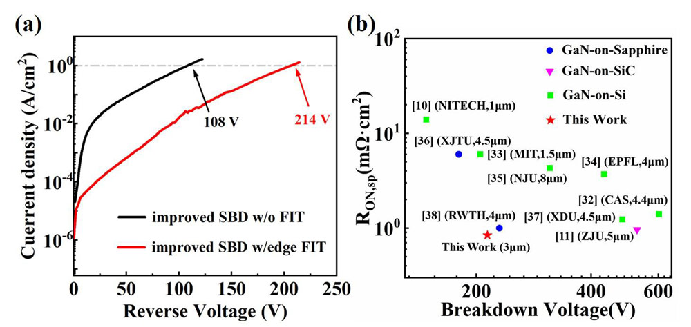
Figure 2: (a) Reverse current-voltage characteristics of improved SBD without FIT and with edge FIT. (b) Benchmark of RON,sp versus BV of fully vertical or quasi-vertical GaN SBDs on foreign substrates.
The researchers report: “The theoretical BV is 221V for a device with the same drift layer (a thickness of 3 μm at a doping concentration of 1.5x10¹⁷/cm3). A slightly lower measured BV of 214V indicates the good crystal quality of the drift layer as well as the effectivity of the edge termination of this work.”
The low resistance compared to other reports of SBDs on foreign (i.e. non-GaN) substrates suggests “good conductivity of the epi-stack”. The team adds: “Much higher BV can be achieved by lowering the n-type doping concentration.” Drift layers in other reports typically have doping concentrations a factor of ten lower.
The author Mike Cooke is a freelance technology journalist who has worked in the semiconductor and advanced technology sectors since 1997.


