


News: Optoelectronics
1 February 2024
Green photonic-crystal surface-emitting lasers
Nichia Corp and Kyoto University in Japan have reported on extending the capability of photonic-crystal surface-emitting lasers (PCSELs) into the green band of the visible spectrum [Natsuo Taguchi et al, Appl. Phys. Express, v17, p012002, 2024].
The researchers describe green PCSEL developments so far as being at a “primitive level” compared with blue PCSELs, or green edge-emitting laser diodes and vertical-cavity surface-emitting laser diodes. However, the team has hopes that such devices could be attractive for materials processing, high-brightness illumination, and display applications.
Photonic crystals (PCs) use two-dimensional lattice structures of different refractive index materials to control optical behavior. One particular hope for PCSELs is to use this control to enable the easier achievement of single-mode behavior at higher output power, improving beam quality.
The researchers comment: “By utilizing a singularity (e.g. Γ) point of the PC, the PCSELs realize both vertical and lateral single-mode oscillation and low-divergence radiation beams with angles of less than 0.2°.” PCSELs could also avoid catastrophic optical damage (COD) from intense light density by spreading the optical power over a larger resonator volume.
The PC was formed in the p-GaN contact layer of the PCSEL epitaxial material, using a silicon dioxide (SiO2) filling material rather than the more usual air of previous studies (Figure 1). By creating the PC after the active layer, the lattice constant (a) of the PC could be adjusted relative to the measured gain wavelength of the active layer of the epitaxial structure.
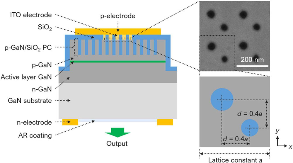
Figure 1: Structure of green-wavelength GaN-based PCSEL: (a) cross-section of diced chip (b) (top) scanning-electron-microscope (SEM) image of PC at p-GaN surface with ITO electrode removed; (bottom) double-lattice PC design scheme.
Filling the lattice with SiO2 avoids current leakage via conductive particles in the sidewalls of the lattice holes, making for more stable current control, and reduced parasitic leakage. The SiO2 also increases the effective refractive index of the PC layer, shifting the guided mode towards the PC and enhancing the coupling with the optical field.
A draw-back of using SiO2 is reduced refractive index contrast with GaN, making the control of the optical waves inside the PC plane more difficult. This was compensated for by increasing the diameter of the holes, and using a double-lattice structure with a unit cell consisting of two holes offset by 0.4a in both the x and y directions. The researchers say that this was “to obtain sufficient in-plane confinement and coupling even in the case of low refractive index contrast between p-GaN and SiO2 filling the PC.”
The PC formation process consisted of depositing indium tin oxide (ITO) transparent conductor on the III-nitride epitaxial material, followed by drilling the PC lattice holes with inductively coupled plasma reactive-ion etch (ICP-RIE) and filling with SiO2 via plasma chemical vapor deposition (CVD). The ITO material was removed from the structure except for a 300μm-diameter circular central region to serve as conduit between the p-electrode and p-GaN.
The researchers report that the SiO2 fill cylinders in the PC contained a small air void in their centers, according to SEM imaging. The team comments: “The shape of the void was uniform within the PC plane, and the presence of the void thus was considered not to significantly impact the behavior of the PCSEL.”
The device was completed by mesa etching down to the n-GaN layer, depositing a SiO2 covering the mesa except for the central ITO region; depositing the p- and n-electrodes to the top and bottom surfaces, respectively; and applying an anti-reflective (AR) coating to the bottom circular laser output region. The devices were diced and flipped onto sub-mounts for performance measurements.
A device with a PC lattice constant a of 210nm achieved around 50mW maximum output with a 5A injection current of 500ns pulses at 1kHz repetition rate. The wall-plug efficiency (WPE) for this was 0.1%. The laser threshold was at 3.89kA/cm2 current density. The slope efficiency was 0.02W/A. The output laser light was linearly polarized with a 0.8 ratio. The divergence angle of the circular far-field pattern (FFP) was of order 0.2°. The laser wavelength was 505.7nm.
A certain amount of tuning of the laser wavelength could be achieved by varying the PC lattice parameter, a, between 210 and 217nm (Figure 2). The maximum emission wavelength, for the 217nm device, was 520.5nm. Since the gain peak of the active layer was around 505nm, lasing was more difficult to achieve at the longer wavelengths, resulting in increased thresholds with the higher PC lattice constants.
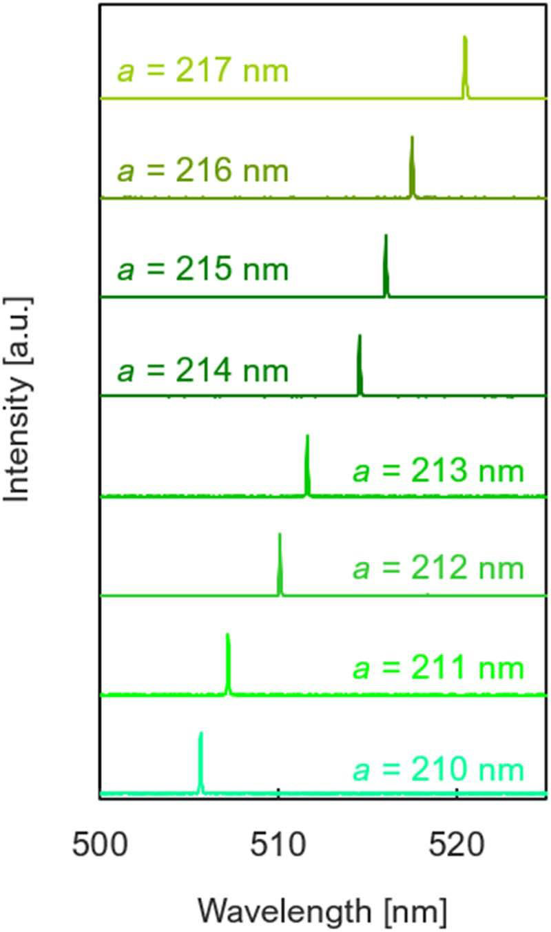
Figure 2: Lasing spectra of devices with different PC lattice constants.
The researchers also report that some of the higher PC lattice constant devices exhibited flat-band lasing with line-shaped FFPs. The team attributed the flat-band lasing to fluctuations in the PC structure and relatively low coupling coefficients with the PC.
The researchers comment: “The WPE can be improved by optimizing both the PC and the epitaxial crystal layers. For the PC, stronger in-plane coupling and vertical radiation are expected to be obtained by optimizing the geometry. The epitaxial crystal layers should be designed to maximize the intensity of the fundamental guided mode in the PC region, while also considering the non-luminescent loss of injected carriers.”
A further desideratum for future research would be to achieve continuous-wave operation.
https://doi.org/10.35848/1882-0786/ad126f
The author Mike Cooke is a freelance technology journalist who has worked in the semiconductor and advanced technology sectors since 1997.


