


News: Microelectronics
5 January 2024
Lateral polarity structure GaN Schottky barrier diodes
Ningbo Institute of Materials Technology and Engineering, and University of Chinese Academy of Sciences in China have reported a high-performance quasi-vertical gallium nitride (GaN) Schottky barrier diode (SBD), using a lateral polarity structure (LPS) with an active III-polar region surrounded by N-polar material [Yijun Dai et al, Appl. Phys. Lett. v123, p252110, 2023].
The resulting devices featured a high 107 on/off current ratio and low leakage under reverse biases up to a 290V breakdown. Vertical GaN SBDs feature low turn-on voltage and high-speed switching characteristics, relative to lateral devices.
The SBD LPS material was grown on 0.5°-misoriented (0001) sapphire (Figure 1). The III-polar active region was grown on a circular patterned aluminium nitride (AlN) nucleation layer. The material grown on bare sapphire was N-polar. The metal-organic chemical vapor deposition (MOCVD) layer sequence consisted of a 3μm buffer layer, a 2μm n+-GaN current-spreading layer, and a 3μm n--GaN drift layer.
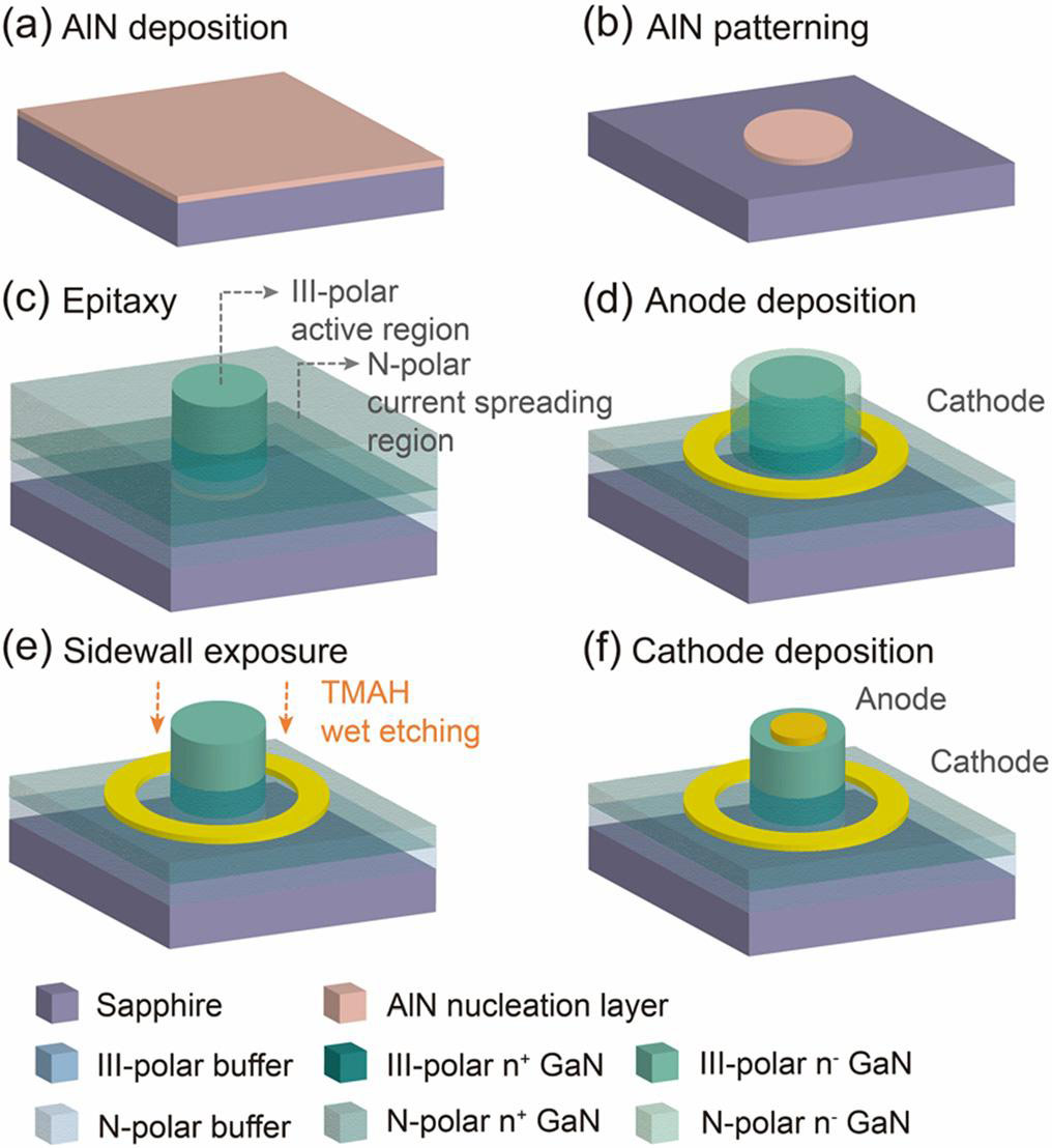
Figure 1: Process scheme for quasi-vertical GaN SBD based on LPS platform.
Fabrication began with plasma etch of the N-polar region down to the current-spreading layer, using a nickel hard mask. This avoided rough N-polar surfaces with hexagonal hillocks that tend to occur in wet etching. An ohmic ring-contact cathode consisting of titanium/aluminium/nickel/gold was deposited using electron-beam evaporation and annealed in nitrogen.
The III-polar mesa sidewall was exposed by selective etching away of the N-polar sheath around the Ga-polar acvtive region with tetramethylammonium hydroxide (TMAH) alkali solution for 20 minutes at 85°C. The OH− ions in the alkali solution interact with the dangling bonds of the surface nitrogen atoms, forming ammonia (NH3) and breaking up the N-polar material. By contrast, with a Ga-polar surface the nitrogen atoms are buried away and it is less easy for the OH− ions to gain access.
The Schottky anode contact, deposited on the drift layer, consisted of nickel/gold. The anode metal contact had a radius of 100μm, while the mesa radius was 110μm. A reference SBD was produced using only plasma etch, but with the same contact structures.
The on/off current ratio of the LPS SBD was of order 107, and the reverse leakage current was reduced by two orders of magnitude relative to the reference device. The ideality factors for the LPS and reference SBDs were 1.03 and 1.09, respectively.
The team comments: “The lower ideality factor for the LPS SBD indicates strong suppression of defect-related leakage paths and recombination centers, which are typically responsible for the non-ideality in GaN diodes.”
The LPS and reference turn-on voltages were 0.5 and 0.6V, respectively. The one area where the LPS device performed less well than the reference was in terms of differential specific on-resistance (Ron): 6.5 for the LPS and 2.1m Ω-cm2 for the reference diodes.
The researchers explain the difference: “The higher Ron value of the LPS SBD can be ascribed to the undercut and wet etching of the N-polar domain beneath the Ohmic contact.”
The Schottky barrier height was extracted using temperature-dependent measurements: 0.82eV for the LPS diode.
The LPS SBD had a 200V higher breakdown voltage (BV) than the reference device: 290V compared with 90V (Figure 2). The peak electric field in the LPS device was estimated at 2.1MV/cm. At 90V, the reverse leakage current in the LPS device was four orders of magnitude smaller than the reference device’s 1A/cm2.
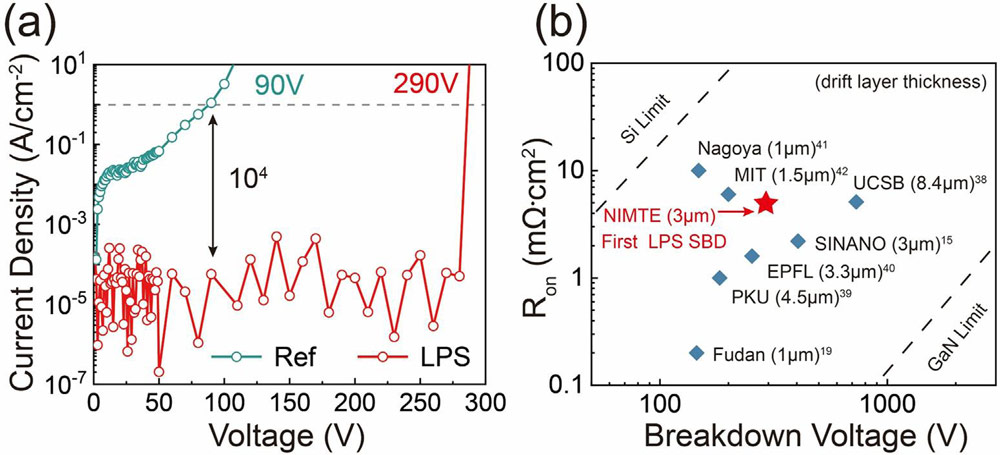
Figure 2: (a) Off-state breakdown characteristics of reference and LPS SBDs. (b) Benchmarks of Ron versus breakdown voltage of LPS device together with other reports.
Further enhancement of breakdown voltage would depend on tackling leakage currents associated with trap-assisted tunneling (TAT) and variable range hopping (VRH). In turn, suppressing these mechanisms would depend on reducing threading dislocations in the active GaN epitaxial layers, which may form a bottleneck on the road to higher BVs in LPS SBDs, according to the team.
The author Mike Cooke is a freelance technology journalist who has worked in the semiconductor and advanced technology sectors since 1997.


