


News: Microelectronics
11 January 2024
Virtual body concept for 650V GaN-on-silicon ICs
Peking University in China has presented a new virtual-body concept for screening p-gate gallium nitride (GaN) high electron-mobility transistor (VB-HEMTs) integrated circuits (ICs) from silicon-substrate-induced cross-talk at the recent IEEE International Electron Devices Meeting (IEDM 2023) in December [Junjie Yang et al, Technical Session 9-6]. The team demonstrated the benefit of using VB-HEMTs in a basic monolithic half-bridge IC.
Although 650V-rated discrete GaN power transistors are commercially available, it is a challenge to boost power densities by fabricating GaN power ICs due to back-gating effects from the substrate. In discrete devices this can be avoided with source-substrate interconnection.
One of the researchers, Jin Wei, an assistant professor at Peking University, comments: “Unfortunately, for the GaN-on-Si platform, if a half-bridge IC is built, there must be at least one of the transistors that fails to have substrate-to-source connection. Thus, the substrate-to-source voltage difference (i.e. back-gating effect) results in a severe dynamic on-resistance RON degradation.”
Although other research teams have reduced the impact on dynamic RON in high-frequency power switching from substrate cross-talk up to 200V by using special substrates, the Peking device uses low-cost standard bulk silicon. The team sees the VB approach as a cost-effective way to boost GaN-on-Si power IC performance to provide a 650V platform based on thick GaN epitaxial films.
The VB-HEMT devices were fabricated using III-N material on 6-inch (150mm)-diameter low-resistivity silicon (Si) wafers (Figure 1). The virtual body material consisted of a 5.2μm buffer, 10nm buried aluminium gallium nitride (Al0.2Ga0.8N), 200nm undoped GaN, 15nm Al0.2Ga0.8N barrier, and 80nm p-GaN gate layers. Conventional devices were also fabricated for comparison, using material without the buried AlGaN layer.
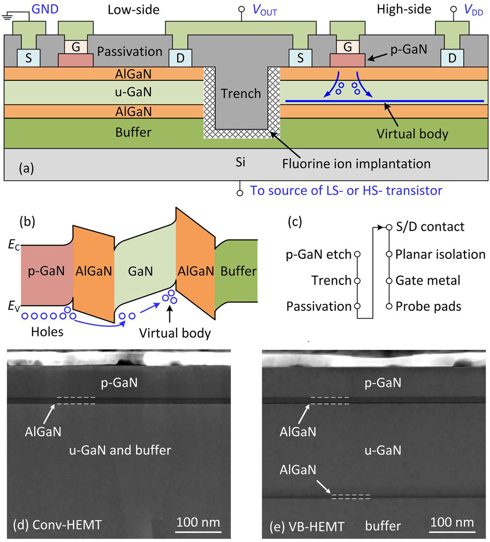
Figure 1: (a) Cross-section of 650V GaN power IC platform. (b) Energy-band diagram in gate region. (c) Process flow for proposed platform. (d, e) Transmission electron microscope (TEM) images of gate region of fabricated (d) conventional- and (e) VB-HEMTs.
The fabrication consisted of gate and 350nm-deep trench etching, 50nm plasma-enhanced chemical vapor deposition (PECVD) silicon dioxide passivation, deposition and annealing of titanium/aluminium/nickel/gold source/drain (S/D) contacts, multi-energy fluorine ion implants, nickel/gold ohmic gate contact deposition and annealing, and contact pad formation.
The VB-HEMT’s ohmic p-GaN gate contact injects holes in the ON-state that accumulate and spread above the buried AlGaN layer to form the virtual body under the two-dimensional electron gas (2DEG) channel near the top AlGaN barrier layer.
The threshold voltage of the VB and conventional HEMTs was 1.4V for 10μA/mm drain current in both devices. The positive threshold means that the devices operate in enhancement-mode (normally-off), as desired for reduced power losses.
The dynamic on-resistance ( RON-dyn) after 650V drain bias stress in the off-state was a factor of 3.66 higher than the static resistance ( RON-stat) in the conventional device. By contrast, the VB-HEMT RON-dyn/ RON-stat factor was as low as 1.28. The VB-HEMT ratio was dependent on the gate potential: 1.28 for 3.5V, but 4.29 for 2V.
The researchers explain the mechanism suppressing RON-dyn in the VB-HEMT: “The buffer trapping is screened by the holes injected from gate and spread along the virtual body. The surface trapping is likely to be mitigated by the recombination of holes from virtual body with electrons from 2DEG, emitting photons to accelerate the recovery of surface trapping.”
Although one might worry that hole injection might increase dynamic OFF-state leakage in the VB-HEMT, the team found that the virtual body mechanism did not in fact increase the OFF current.
In the half-bridge configuration, the VB suppresses cross-talk between the transistors by shielding the channel from the back gate effect of the silicon substrate. With conventional HEMTs, if the low-side transistor’s source contact is connected to the substrate this induces a negative back gate on the high-side device. Connection of the substrate to the high-side source produces a negative gate effect on the low-side device. Both these effects impact performance, increasing the RON, and hence increasing power loss.
The team confirmed VB screening from substrate back-gating effects by biasing the substrate with 10kHz pulses of ±400V and determining the RON of a half-bridge IC at various gate potentials (Figure 2). The high-side drain was connected to a 3V VDD power supply through a 300Ω load resistor. The low-side source was connected to ground. Various gate potentials (VGS) were used.
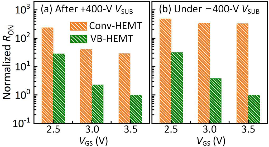
Figure 2: Performance of conventional and VB HEMTs: normalized RON (a) after +400V and (b) during −400V VSUB biases.
Since the half-bridge ( RON) was connected in series with the load (RL), RON = RLVDS/(VDD−VDS), where VDS was the measured voltage across the half-bridge. The performance of the VB-HEMT device was not impacted by the substrate stresses when the gate was at 3.5V, unlike with conventional p-gate HEMTs.
The author Mike Cooke is a freelance technology journalist who has worked in the semiconductor and advanced technology sectors since 1997.


