


News: Microelectronics
18 January 2024
UCSB reports first N-polar InAlGaN HEMT
University of California Santa Barbara (UCSB) in the USA has reported the first N-polar indium aluminium gallium nitride (InAlGaN) quaternary back-barrier high-electron-mobility transistor (HEMT) [Robert Hamwey et al, IEEE Electron Device Letters, published online 25 December 2023].
The advantages of growing III-N heterostructures for HEMTs with AlGaN ternary barriers in the N-polar direction have included record high output power, power density, and power-added efficiency at 94GHz, compared with devices based on the more usual Ga-polar structure. The use of quaternary InAlGaN enables high Al content without increasing the strain due to lattice mismatching. AlGaN suffers from an upper limit in Al concentration before cracking occurs.
The epitaxial structure for the HEMT was grown by metal-organic chemical vapor deposition (MOCVD) on 4°-miscut sapphire (Al2O3) substrate (Figure 1). Such substrates are used to avoid hexagonal hillock defect formation, which commonly occur in N-polar growth. Iron (Fe) doping created a semi-insulating GaN buffer layer, before an unintentionally doped (UID) layer. The channel of the device consisted of a two-dimensional electron gas (2DEG), which formed in the GaN channel layer near the AlN spacer and InAlGaN back-barrier layers. The back barrier was grown at 910°C. The material was capped with 5nm silicon nitride (SiNx) for protection before HEMT fabrication processing.
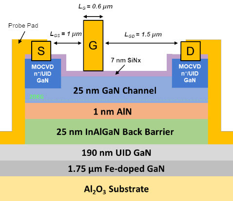
Figure 1: Planar HEMT device structure.
The UCSB team points out three advantages arising from the N-polar orientation: “(i) improved carrier confinement of the 2DEG with a wide-bandgap back barrier, (ii) direct access from the source and drain contacts to the GaN channel, rather than through a wide-bandgap barrier, which leads to a decreased 2DEG contact resistance, and (iii) the ability to achieve a shorter gate-to-2DEG distance by reducing the channel layer thickness rather than the barrier layer thickness.”
Materials analysis after growth suggested that the first few nanometers of InAlGaN had graded Ga content, while the main body was In0.12Al0.73Ga0.15N. The lattice mismatch was estimated to be 0.44%.
Room-temperature Van der Pauw Hall measurements gave a 2DEG sheet carrier density (ns) of 2.85x10¹³/cm2, a mobility of 1048cm2/V-s, and an isotropic sheet resistance of 209Ω/square. The team comments: “We believe that the large 2DEG density is a result of the relatively thick channel and barrier layers, as well as the ionization of hole traps at the net negatively polarized barrier/buffer interface.”
Patterning for the HEMT fabrication used an i-line stepper. The source and drain contact regions consisted of MOCVD-regrown n+-doped/UID GaN with nickel/gold metal electrodes. The gate metal–insulator–semiconductor (MIS) gate stack used MOCVD SiNx as the dielectric insulation and nickel/gold as the metal. Nickel/gold was also used for probe pads.
The source-drain direction was oriented parallel to the <11–20> direction of the crystal structure. The substrate miscut was such that steps formed along this direction. The researchers comment: “This choice was made considering previous work which showed superior conductivity for devices with electron transport aligned parallel to the surface steps.” In fact, measurements along the step direction gave a sheet resistance of 179Ω/square, lower than the isotropic value. The calculated mobility in this direction was estimated to be 1225cm2/V-s.
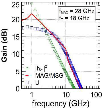 Figure 2: Intrinsic HEMT small-signal response at peak fmax bias (−9V gate, 5V drain).
In DC measurements the HEMTs demonstrated a peak drain current (ID) of 1.92A/mm and an on-resistance of 0.62Ω-mm at 0V gate potential. The threshold voltage (VTH) was −10.6V (normally-on, depletion-mode). The large value of |VTH| is attributed to the large ns, requiring a large gate potential to deplete the carrier concentration and switch off current flow between the source and drain. Other reports of AlGaN/GaN N-polar HEMTs typically have |VTH|<10V. For many applications a “normally-off” (enhancement-mode) behavior with positive VTH is preferred.
The peak transconductance (gm) was 212mS/mm. The researchers report that their device demonstrates 31% and 66% increases over N-polar InAlN/GaN HEMTs of similar dimensions in peak ID and peak gm, respectively.
The frequency performance was measured in the range 0.5–67GHz (Figure 2). The researchers extracted current-gain cut-off (fT) and power-gain cut-off (fmax) frequencies of 18GHz and 28GHz, respectively.
The author Mike Cooke is a freelance technology journalist who has worked in the semiconductor and advanced technology sectors since 1997.


