


News: Suppliers
17 July 2024
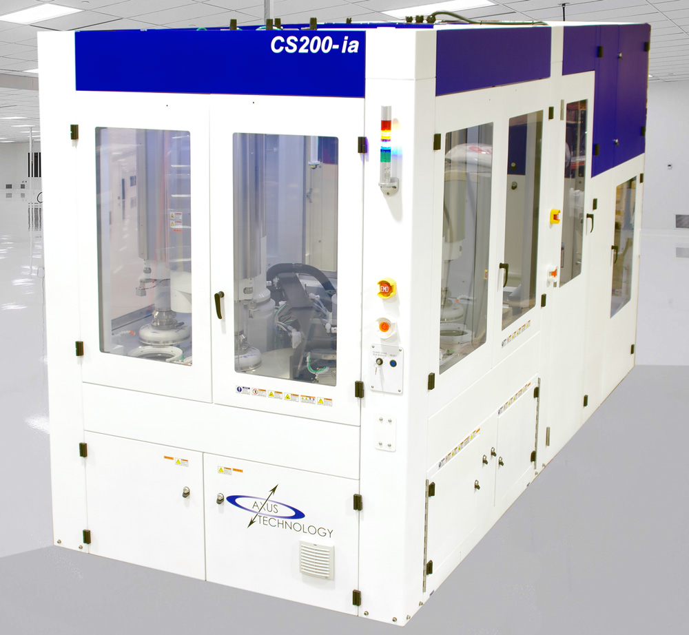
Axus wins orders for Capstone CMP system from SiC device makers
Axus Technology of Chandler, AZ, USA – a provider of chemical-mechanical planarization (CMP), wafer thinning and surface-processing solutions – has reported strong sales momentum for its Capstone CS200 Series of CMP processing tools. In recent months, the firm has received orders from silicon carbide (SiC) semiconductor makers in Europe, Asia and North America.
Underscoring the platform’s flexibility and breadth of capabilities, the Capstone orders include R&D/engineering and production-ready tools, with the latter configured for volume production of both 150mm and 200mm wafers. Built using flexible technology, Capstone is claimed to be the first new 150/200mm CMP platform brought to market in more than three decades and the first that can process two different wafer sizes simultaneously, enabling the tool to deliver industry-high throughput and yields.
Since introducing the Capstone platform in 2020, Axus has built on its range, introducing SiC-optimized wafer carriers and achieving processing milestones. The latest Capstone CS200-ia configuration integrates the firm’s Aquarius wafer cleaning system to enable advanced CMP and post-CMP cleaning in a single system.
“Many of our customers represent the top tier of SiC device and/or wafer manufacturers worldwide,” says Axus’ director of process technology Catherine Bullock. “These customers have conducted extensive process and equipment testing to thoroughly characterize and compare various solutions for advanced SiC CMP,” she adds. “All of them selected Capstone as their preferred platform. This is particularly relevant given the significant challenges and differentiation associated with CMP for SiC as compared to more mature CMP applications.”
Capstone differentiators
Axus claims that Capstone offers several differentiating competitive advantages that are driving its growth in SiC CMP, including:
- a flexible architecture that can process up to four wafers simultaneously and provides both the highest throughput and the smallest footprint, minimizing overall cost of ownership (CoO);
- fully integrated, advanced post-CMP cleaning, which enables single-pass processing for both polish and clean, eliminating the need for additional post-process wafer handling, downstream process steps, and fab equipment;
- process temperature control technology that enables higher-pressure/velocity process conditions – delivering higher removal rates, higher throughput, and lower cost of consumables to substantially improve overall CoO; and
- a considerable reduction in energy and resource consumption, lowering operating and facilities costs while improving environmental sustainability.
“Silicon carbide is growing at a rapid pace – much faster than CMOS – fueled by demand for power electronics applications such as AI data centers, renewable energy and EVs,” notes CEO Dan Trojan. “With our SiC engineering brain trust, proven product portfolio in CMP and related technologies, and growing base of leading suppliers and SiC customers – evidenced by this recent order influx – Axus Technology is well positioned to become the industry leader in CMP for compound semiconductors,” he reckons.
Axus says that it is consulting with developers of SiC and other compound semiconductor devices to help them determine their optimal path for scaling from 150mm to 200mm production. With its recent infusion of capital funding, the company is stepping up its focus on scaling to high-volume manufacturing, enabling the company and its customers to collaborate on go-forward strategies.
Axus secures $12.5m in funding from IntrinSiC


