


News: Microelectronics
18 July 2024
TMAl reflow GaN-on-silicon for fully vertical electronics
École Polytechnique Fédérale de Lausanne (EPFL) in Switzerland claims the first demonstration of direct growth of gallium nitride (GaN) at high temperature on silicon (Si) substrates simply by using a trimethyl-aluminium (TMAl) preflow, without any intentional AlN buffer [Alessandro Floriduz et al, Jpn. J. Appl. Phys., v63, p060904, 2024].
Among the benefits of the process could be the realization of “more efficient fully vertical GaN-on-Si devices, in which the silicon substrate may become a functional part of the device, as well as novel devices that require effective current conduction to the substrate,” according to the team.
Vertical current flow diode/transistor devices are particularly sought for power electronics, and the GaN/Si combination could promote both high-power performance and low production cost.
The researchers comment: “For GaN-on-Si devices, a fully vertical structure (where current flows vertically through electrodes located on opposite sides of the wafer) is preferable, to avoid current crowding and achieve low on-state resistance.”
While fully vertical GaN devices have been demonstrated on silicon, the substrate and low-conduction buffer layers usually need to be removed, increasing production cost and hindering commercial adoption.
Unfortunately, the conventional GaN/Si process uses an AlN interlayer, which is usually highly insulating due to the 6eV energy gap between the conduction and valence bands.
The EPFL team prepared samples using metal-organic chemical vapor deposition (MOCVD) on 2-inch Si(111) n-type phosphorus-doped wafers. The researchers compared the use of a TMAl preflow against the conventional growth of an AlN interlayer on silicon before GaN epitaxy.
The difference in growth conditions was that during the preflow the line from the nitrogen precursor, ammonia (NH3), was shut off. It was only when the the TMAl line was shut off that the NH3 and TMGa supplies were opened and the GaN growth began. The resulting GaN layers were Ga-polar, as confirmed by non-etching in potassium hydroxide solution.
The main control variable was the durations of the steps. The temperature and pressure during the preflow and GaN growth were 925°C and 50mbar, respectively. The carrier gas was hydrogen. The AlN growth was at the higher temperature of 1000°C. The silicon wafer was prepared for the MOCVD by thermal cleaning at 100mbar pressure, and 1000/1050°C for preflow/AlN interlayer, respectively. The GaN layers were doped with silicon, targeting an electron concentration around 4x10¹⁸/cm3.
The GaN layer thickness was 110nm to avoid cracking on the thickest 100nm AlN interlayer grown. The GaN growth resulted in single-crystal material in all cases.
Optical microscope inspection showed a rough surface in the cases of thin 3nm AlN interlayer and for short TMAl preflow of 5 seconds. Also, the longest 30s TMAl preflow sample showed degradation towards the wafer edge, which the team attributes to “an excessive accumulation of Al on the wafer surface due to the longer preflow, leading to meltback etching of the silicon wafer, initiated by Si–Al reactions. This accumulation occurs at the wafer periphery due to the horizontal reactor design (single 2-inch wafer carrier with rotation) and the low gas velocity during preflow.”
Atomic force microscope (AFM) investigation showed that the preflow method resulted in smoother GaN surfaces than the best AlN interlayer. The 15s and 30s preflows root-mean-square roughness values were both of the order of 1nm, with no observable holes in the GaN layer. The very short 5s preflow gave a very rough surface of 23nm, larger than those with AlN interlayer (1.5nm for 100nm, 3nm for 3nm).
The x-ray diffraction (XRD) rocking curve (XRC) scans were collected from the 002 and 102 planes (Figure 1). The researchers report: “Narrower XRC peaks were obtained in GaN samples directly grown with the TMAl preflow, indicating an improved crystalline quality compared to the use of conventional AlN buffers.”
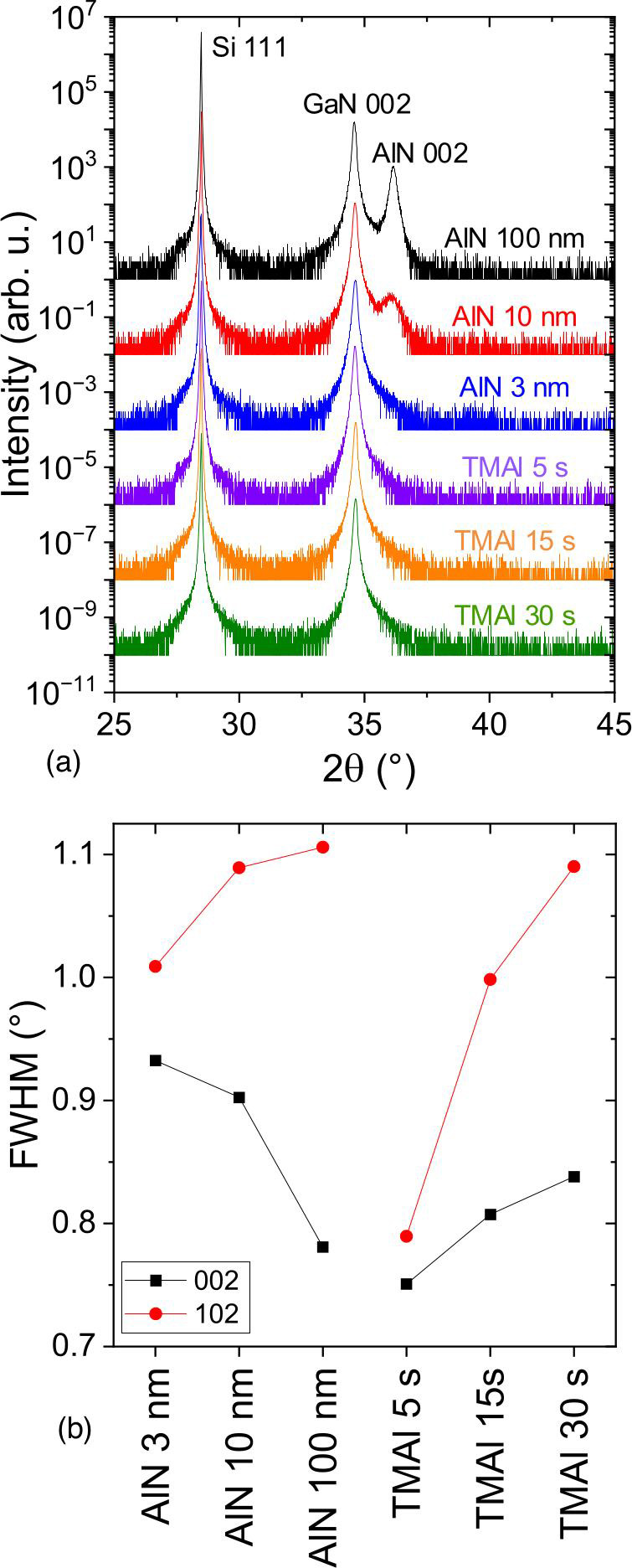
Figure 1: (a) Symmetric 2θ-ω XRD scans and (b) FWHM values of XRCs for GaN 002 and GaN 102 diffraction peaks.
The full-width at half-maximum (FWHM) of the 002 peak is sensitive to the presence of screw and mixed dislocations, while the 102 scans give information on edge dislocations. Although the 5s preflow was apparently more crystalline, the lack of edge dislocations was related to the lack of coalescence of the GaN epitaxial layer, resulting in a rough surface with holes.
The researchers comment: “Increasing the TMAl preflow time to 15s and 30s resulted in fully coalesced samples, which consequently exhibited broader GaN 102 peaks.”
The researchers add: “By optimizing the preflow time, the direct high-temperature growth of GaN on Si with a TMAl pre-treatment not only successfully results in a fully coalesced surface without traces of meltback etching, but it also greatly improves the GaN surface morphology and its crystal quality compared to using AlN buffers.”
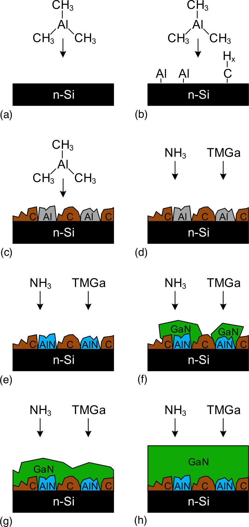
Figure 2: Suggested growth mechanisms: (a–c) Preflow deposition of Al and C. (d–e) Nitridation of Al during early GaN step. (f) 3D GaN growth on AlN regions. (g) Coalescence. (h) 2D layer-by-layer growth.
The researchers suggest (Figure 2) that the preflow step creates a surface layer consisting of Al and carbon (C, from the ‘organic’ part of the MOCVD), and compounds such as aluminium carbide (Al4C3). When the ammonia flow starts during the GaN growth the Al is nitrided to AlN and acts as a nucleation point for GaN crystal growth in a 3D mode. The C-containing regions act as nanomasks, “favoring lateral growth, as well as dislocation bending and annihilation (analogously to epitaxial lateral overgrowth).” When the GaN islands coalesce the growth transitions to a 2D mode.
The researchers also measured the current flow across the Si/GaN interface under bias with a view to fully vertical electronic device structures (Figure 3). Clearly, the preflow technique resulted in much higher current (~3 orders of magnitude) under forward and reverse bias than even the thinnest 3nm AlN interlayer. The small conduction-band energy difference of 0.3eV gives an asymmetric current response to a bias (around three orders of magnitude at larger biases).
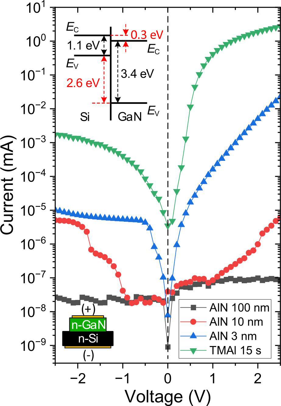
Figure 3: Current–voltage (I–V) measurements of n-GaN/n-Si heterostructures, directly grown with 15s TMAl preflow (green), and with conventional AlN buffers. Forward bias refers to positive voltage applied to n-GaN (bottom-left inset). Top-left inset schematically represents band alignment of GaN and Si.
The electrodes used in these measurements were chromium/gold on the GaN layer, and indium on the silicon wafer backside.
The author Mike Cooke is a freelance technology journalist who has worked in the semiconductor and advanced technology sectors since 1997.


