


News: Microelectronics
25 July 2024
German researchers demo practical implementation of AlN-based value chain for power semiconductors
In power electronics, conventional silicon devices are being replaced by more powerful wide-bandgap (WBG) semiconductors with superior physical and electrical properties. Silicon carbide (SiC) has already established itself on an industrial scale, but devices based on gallium nitride (GaN) are also on the rise. However, it is already foreseeable that, in the future, even WBG device properties will be surpassed by ultrawide-bandgap (UWBG) semiconductors like aluminium nitride (AlN).
Devices fabricated on single-crystal AlN wafers can achieve a higher power density and efficiency compared with GaN technology. They also exhibit lower dynamic parasitic effects and higher reliability. At the same time, the high thermal conductivity of AlN enables good heat dissipation of the devices. Semiconductor technology based on AlN for power electronic transistors as well as millimeter-wave radio-frequency circuits hence has the potential to significantly reduce losses in electrical energy conversion and high-frequency transmission.
Establishing an AlN process chain in Germany
To make AlN technology accessible to industry in the medium term, the related existing activities in Germany have been combined in a strategic cluster. The aim is to establish a German value chain for AlN-based technology and to establish international leadership in this increasingly economically important field. Berlin-based Ferdinand-Braun-Institut, Leibniz-Institut für Höchstfrequenztechnik (FBH), the Erlangen-based Fraunhofer IISB (Institute for Integrated Systems and Device Technology) and III/V-Reclaim PT GmbH are collectively driving the initiative. They span the entire value chain, starting with the growth of AlN crystals using physical vapor transport (PVT), to wafering and polishing of epi-ready AlN-wafers, and the epitaxy of the functional device layers, up to the fabrication of transistors for power electronics and millimeter-wave applications.
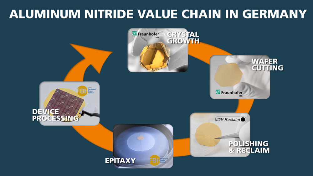
Picture: © Fraunhofer IISB/Elisabeth Iglhaut.
The consortium has now successfully demonstrated the practical implementation of a value chain for AlN devices for the first time in Germany and Europe. To this end, AlN crystals were grown at Fraunhofer IISB and sliced into AlN wafers with a diameter up to 1.5-inches. III/V-Reclaim has developed a polishing process for epitaxial wafer production. Functional epitaxial layers were then applied to these wafers at the FBH, and AlN/GaN high-electron-mobility transistors (HEMTs) were successfully processed on them.
The first transistor generations produced with these wafers already show promising electrical properties, such as a breakdown voltage of up to 2200V and a power density superior to SiC as well as GaN-based power-switching devices.
Investment for the future
Targeting ever higher energy efficiency and progressive miniaturization is crucial for power electronic systems and in microwave communication. However, the static and dynamic conduction losses in the semiconductor materials unnecessarily increase the switching losses in supply, distribution and usage of electrical energy. This results in higher consumption of primary energy. In Europe alone, conversion losses waste several terawatt-hours of electrical energy per year, and the trend is for this to increase. To achieve significant energy savings, the semiconductor material itself must be addressed.
Compared with established silicon devices, AlN/GaN HEMTs — now successfully produced on AlN wafers — offer up to 3000 times less conduction losses than with silicon and are about ten times more efficient than SiC transistors.
The research was supported by funding from the German Federal Ministry of Education and Research (BMBF) within the ForMikro-LeitBAN and Nitrides-4-6G projects.
FBH-led project ‘power transistors based on AlN (ForMikro-LeitBAN)’ launched


