


News: Suppliers
26 July 2024
Comparison between MBE and MOCVD technologies
Both molecular beam epitaxy (MBE) and metal-organic chemical vapour deposition (MOCVD) reactors operate in cleanroom environments and use the same set of metrology tools for wafer characterization. Solid-source MBE uses high-purity, elemental precursors heated in effusion cells to create a molecular beam to enable deposition (with liquid nitrogen used for cooling). In contrast, MOCVD is a chemical vapor process, using ultra-pure, gaseous sources to enable deposition, and requires toxic gas handing and abatement. Both techniques can produce identical epitaxy in some material systems, such as arsenides. The choice of one technique over the other for particular materials, processes, and markets is discussed.
Molecular beam epitaxy
An MBE reactor typically comprises a sample transfer chamber (open to the air, to allow wafer substrates to be loaded and unloaded) and a growth chamber (normally sealed, and only open to the air for maintenance) where the substrate is transferred for epitaxial growth. MBE reactors operate in ultra-high vacuum (UHV) conditions to prevent contamination from air molecules. The chamber can be heated to accelerate the evacuation of these contaminants if the chamber has been open to air.
Often, the source materials of epitaxy in an MBE reactor are solid semiconductors or metals. These are heated beyond their melting points (i.e. source material evaporation) in effusion cells. Here, atoms or molecules are driven into the MBE vacuum chamber through a small aperture, which gives a highly directional molecular beam. This impinges on the heated substrate; usually made of single-crystal materials like silicon, gallium arsenide (GaAs) or other semiconductors. Providing that the molecules do not desorb, they will diffuse on the substrate surface, promoting epitaxial growth. The epitaxy is then built-up layer by layer, with each layer’s composition and thickness controlled to achieve the desired optical and electrical properties.
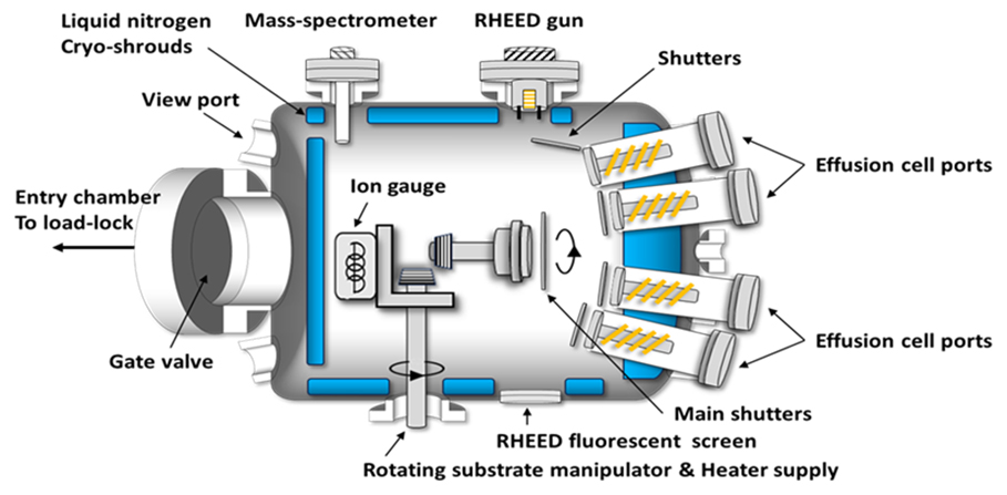
The substrate is mounted centrally, within the growth chamber, on a heated holder surrounded by cryoshields, facing the effusion cells and shutter system. The holder rotates to provide uniform deposition and epitaxial thickness. The cryoshields are liquid-nitrogen cooled-plates which trap contaminants and atoms in the chamber that are not previously captured on the substrate surface. The contaminants can be from desorption of the substrate at high temperatures or by ‘over filling’ from the molecular beam.
The ultra-high-vacuum MBE reactor chamber enables in-situ monitoring tools to be used to control the deposition process. Reflection high-energy electron diffraction (RHEED) is used for monitoring the growth surface. Laser reflectance, thermal imaging, and chemical analysis (mass spectrometry, Auger spectrometry) analyse the composition of the evaporated material. Other sensors are used to measure temperatures, pressures and growth rates in order to adjust process parameters in real-time.
Growth rate and adjustment
The epitaxial growth rate, which is typically about a third of a monolayer (0.1nm, 1Å) per second, is influenced by the flux rate (the number of atoms arriving at the substrate surface, controlled by the source temperature) and the substrate temperature (which affects the diffusive properties of atoms on the substrates surface and their desorption, controlled by the substrate heat). These parameters are independently adjusted and monitored within the MBE reactor, to optimize the epitaxial process.
By controlling growth rates and the supply of different materials using a mechanical shutter system, ternary and quaternary alloys and multi-layer structures can be grown reliably and repeatedly. After deposition, the substrate is cooled down slowly to avoid thermal stress and tested to characterize its crystalline structure and properties.
Material characteristics for MBE
The characteristics of III-V material systems used in MBE are:
- Silicon: Growth on silicon substrates requires very high temperatures to ensure oxide desorption (>1000°C), so specialist heaters and wafer holders are required. Issues around the mismatch in lattice constant and expansion coefficient make III-V growth on silicon an active R&D topic.
- Antimony: For III-Sb semiconductors, low substrate temperatures must be used to avoid desorption from the surface. ‘Non-congruence’ at high temperatures may also occur, where one atomic species may be preferentially evaporated to leave non-stoichiometric materials.
- Phosphorus: For III-P alloys, phosphorous will be deposited on the inside of the chamber, requiring a time-consuming clean-up process which may make short production runs unviable.
- Strained layers, which generally require lower substrate temperatures to reduce the surface diffusion of atoms, reducing the likelihood of a layer relaxing. This can lead to defects, as the mobility of deposited atoms reduces, leaving gaps in the epitaxy which may become encapsulated and cause failure.
Metal-organic chemical vapour deposition
The MOCVD reactor has a high-temperature, water-cooled reaction chamber. Substrates are positioned on a graphite susceptor heated by either RF, resistive or IR heating. Reagent gases are injected vertically into the process chamber above the substrates. Layer uniformity is achieved by optimizing temperature, gas injection, total gas flow, susceptor rotation and pressure. Carrier gases are either hydrogen or nitrogen.
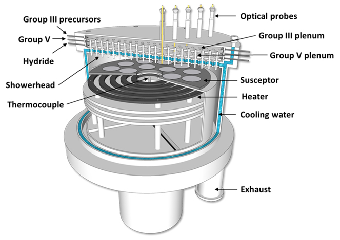
To deposit epitaxial layers, MOCVD uses very high-purity metal-organic precursors such as trimethylgallium for gallium or trimethylaluminium for aluminium for the group-III elements and hydride gases (arsine and phosphine) for the group-V elements. The metal-organics are contained in gas flow bubblers. The concentration injected into the process chamber is determined by temperature and pressure of the metal-organic and carrier gas flow through the bubbler.
The reagents fully decompose on the substrate surface at the growth temperature, releasing metal atoms and organic by-products. The concentration of reagents is adjusted to produce different, III-V alloy structures, along with a run/vent switching system for adjusting the vapour mixture.
The substrate is usually a single-crystal wafer of a semiconductor material such as gallium arsenide, indium phosphide, or sapphire. It is loaded onto the susceptor within the reaction chamber over which the precursor gases are injected. Much of the vapourized metal-organics and other gases travel through the heated growth chamber unaltered, but a small amount undergoes pyrolysis (cracking), creating subspecies materials that absorb onto the surface of the hot substrate. A surface reaction then results in the incorporation of the III-V elements into an epitaxial layer. Alternatively, desorption from the surface may occur, with unused reagents and reaction products evacuated from the chamber. Additionally, some precursors may induce ‘negative growth’ etching of the surface, such as in carbon doping of GaAs/AlGaAs, and with dedicated etchant sources. The susceptor rotates to ensure consistent composition and thicknesses of the epitaxy.
The growth temperature required in the MOCVD reactor is primarily determined by the required pyrolysis of the precursors, and then optimized regarding surface mobility. The growth rate is determined by the vapour pressure of the group-III metal-organic sources in the bubblers. Surface diffusion is affected by atomic steps on the surface, with misoriented substrates often being used for this reason. Growth on silicon substrates requires very high-temperature stages to ensure oxide desorption (>1000°C), demanding specialist heaters and wafer substrate holders.
The reactor’s vacuum pressure and geometry means that in-situ monitoring techniques vary to those of MBE, with MBE generally having more options and configurability. For MOCVD, emissivity-corrected pyrometry is used for in-situ, wafer surface temperature measurement (as opposed to remote, thermocouple measurement); reflectivity allows surface roughening and the epitaxial growth rate to be analysed; wafer bow is measured by laser reflection; and supplied organometallic concentrations can be measured via ultrasonic gas monitoring, to increase the accuracy and reproducibility of the growth process.
Typically, aluminium-containing alloys are grown at higher temperatures (>650°C), while phosphorous-containing layers are grown at lower temperatures (<650°C), with possible exceptions for AlInP. For AlInGaAs and InGaAsP alloys, used for telecoms applications, the difference in the cracking temperature of arsine makes the process control simpler than for phosphine. However, for epitaxial re-growth, where the active layers are etched, phosphine is preferred. For antimonide materials, unintentional (and generally unwanted) carbon incorporation into AlSb occurs, due to the lack of an appropriate precursor source, limiting the choice of alloys and so the uptake of antimonide growth by MOCVD.
For highly strained layers, due to the ability to routinely utilize arsenide and phosphide materials, strain balancing and compensation are possible, such as for GaAsP barriers and InGaAs quantum wells (QWs).
Summary
MBE generally has more in-situ monitoring options than MOCVD. The epitaxial growth is adjusted by the flux rate and substrate temperature, which are separately controlled, with associated in-situ monitoring allowing a much clearer, direct, understanding of the growth processes.
MOCVD is a highly versatile technique that can be used to deposit a wide range of materials, including compound semiconductors, nitrides and oxides, by varying the precursor chemistry. Precise control of the growth process allows the fabrication of complex semiconductor devices with tailored properties for applications in electronics, photonics and optoelectronics. MOCVD chamber clean-up times are quicker than MBE.
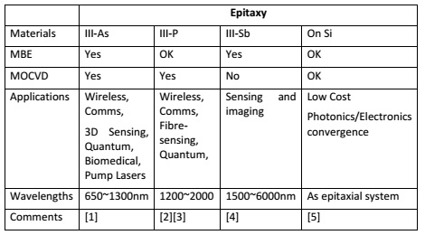
Material choices: MBE and MOCVD.
[1] Quantum dot lasers made using MBE extend the wavelength options from ~1100nm to ~1300nm.
[2] MBE growth on InP substrates is routine, but the deposition of phosphorous materials requires a chamber clean-up process before opening the chamber safely.
[3] Epitaxial regrowth via MOCVD is routine, with multiple steps possible.
[4] Significant carbon incorporation in AlSb has limited Sb epitaxy options via MOCVD, with MBE being dominant.
[5] Special, high-temperature heating elements are required to desorb native oxide on silicon, so this is not viable for MBE or MOCVD.
MOCVD is excellent for the regrowth of distributed feedback (DFBs) lasers, buried heterostructure devices, and butt-jointed waveguides. This may include in-situ etching of the semiconductor. MOCVD is, therefore, ideal for monolithic InP integration. Although monolithic integration in GaAs is in its infancy, MOCVD enables selective area growth, where dielectric masked areas help space the emission/absorption wavelengths. This is difficult to do with MBE, where polycrystal deposits can form on the dielectric mask.
In general, MBE is the growth method of choice for Sb materials and MOCVD is the choice for P materials. Both growth techniques have similar capabilities for As-based materials. Traditional MBE-only markets, such as electronics, can now be served equally well with MOCVD growth. However, for more advanced structures, such as quantum dot and quantum cascade lasers, MBE is often preferred for the base epitaxy. If epitaxial regrowth is required, then MOCVD is generally preferred, due to its etching and masking flexibility.
III-V Epi’s 2023 growth driven by industrial projects comprising 70% of revenue
III-V Epi’s CTO Richard Hogg being made Professor of Photonics at Aston University


