


News: LEDs
11 July 2024
Red InGaN micro-LED on silicon prospecting
Researchers based in Korea report on size-dependent characteristics of indium gallium nitride (InGaN) red micro-scale light-emitting diodes (micro-LEDs) fabricated on 4-inch silicon (Si) substrates [Juhyuk Park et al, Optics Express, v32, p24242, 2024].
The team from Korea Advanced Institute of Science and Technology (KAIST), Korea Advanced Nano Fab Center (KANC), and Chungbuk National University, sees its work as being pioneering, adding: “This work is the first investigation into the size-dependent characteristics of InGaN/GaN red micro-LEDs grown on Si substrates with dimensions under 100μm.”
LED arrays based on the devices reached resolution as high as 4232 pixels per inch (PPI). Relatively poor red LED performance is a roadblock on the route to full-color displays based on InGaN LED technology. Apart from much lower cost, the advantage of using silicon substrates include better thermal conductivity than the more usual sapphire-based epitaxy.
The epitaxial structure for the red micro-LED arrays was grown by metal-organic chemical vapor deposition (MOCVD) on 4-inch Si (111) wafers (Figure 1). The buffer region was 1.3μm, followed by 2μm n-GaN contact. The superlattice consisted of 10 pairs of 0.9/5nm Al0.04Ga0.96N/In0.05Ga0.95N.
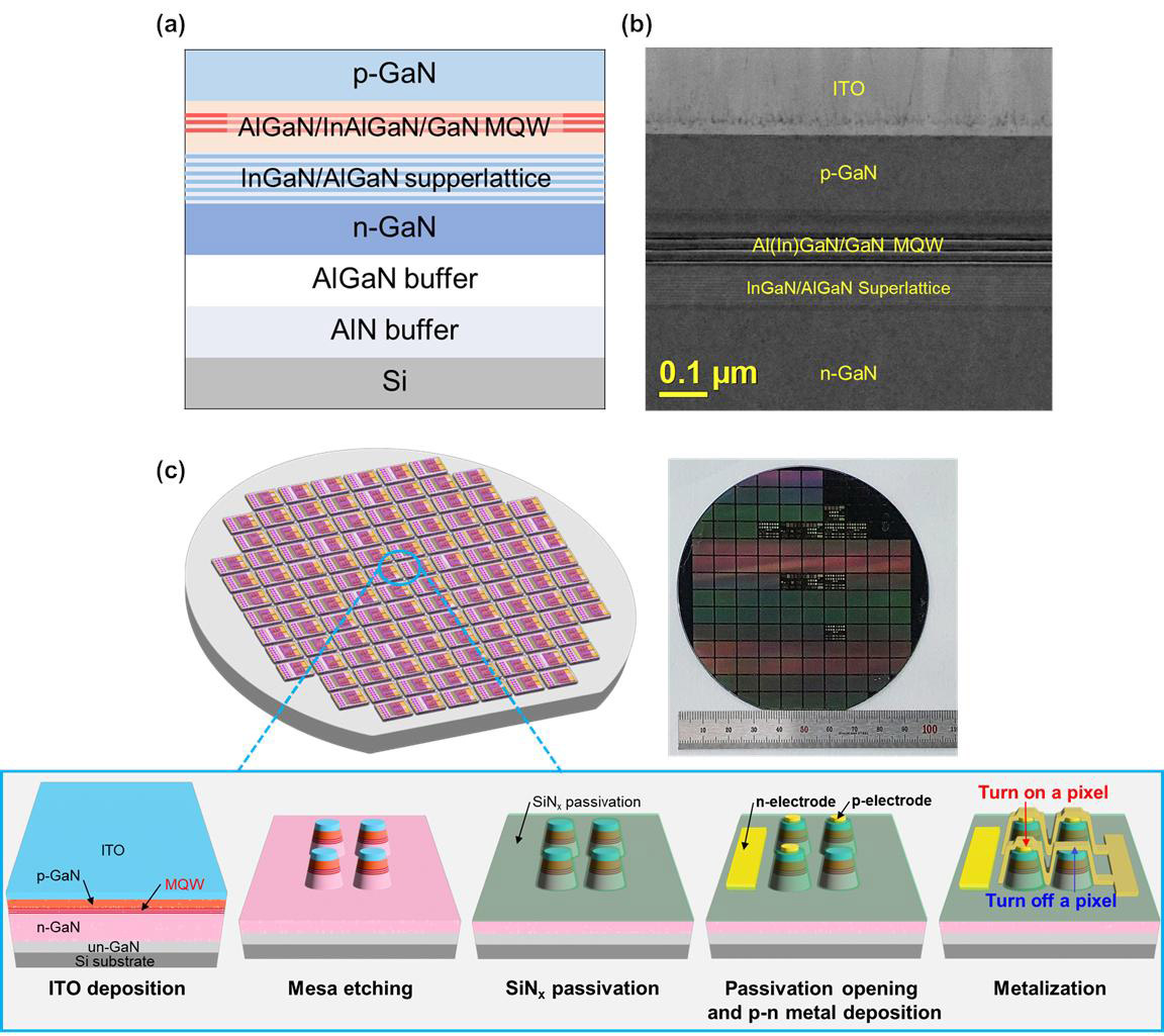
Figure 1: (a) InGaN/GaN red micro-LED epitaxial structure. (b) Transmission electron microscope (TEM) image. (c) Fabrication process flow and photograph inset of InGaN/GaN red micro-LEDs on 4-inch silicon wafer.
The active light-generating region consisted of a three-well multiple quantum well (MQW). The wells were 2.4nm In0.23Al0.05Ga0.72N separated by 10nm GaN barriers. The MQW was capped with 12nm AlGaN varying in Al-content in three steps (13%, 7%, 42%). The structure was completed with 150nm p-GaN as the contact layer.
The researchers used the material to fabricate the red micro-LED arrays. The first step was deposition of 200nm annealed indium tin oxide (ITO) as a transparent ohmic conductor p-electrode. The mesa structures for the individual LEDs were fabricated through a three-step inductively coupled plasma-reactive ion etching process. The steps consisted of ITO etching, hydrochloric acid treatment to remove ITO residues, and the final etching down to the n-GaN layer.
The metal contacts with the common n-electrode and ITO p-contact consisted of chromium/gold (Cr/Au), deposited after 500nm silicon nitride (SiNx) CVD passivation. A passive matrix (PM) array format was used to wire the LEDs together in pixels.
The researchers point out that all these processes were carried out at the 4-inch wafer scale. The team comments: “In semiconductor fabrication, the most effective way to lower costs is through large-scale wafer-level fabrication, as it allows for the production of a larger number of devices in a single process.”
The dark current density under reverse bias was below 1μA/cm2 for all devices sizes from 5μm to 100μm.
The LEDs suffered a blue-shift in wavelength as the injection current density increased. For arrays of 12μm LEDs, the wavelength shifted from 648nm to 624nm for injections between 3A/cm2 and 30A/cm2, respectively. Standard red 642nm emission occurred at 5A/cm2.
The full-width at half maximum (FWHM) for the LEDs was around 65nm at low injection, narrowing to 50nm at 30A/cm2. This put a large chunk of the emissions in the ‘orange’ range (590–625nm) rather than ‘red’ (625–750nm).
The researchers comment: “The peak wavelength shift in InGaN quantum wells was attributed to the quantum-confined Stark effect (QCSE) and the band-filling effect.”
The QCSE results from shifts in the energy levels due to the different combinations of applied electric field and electric fields arising from the strain-dependent contrasts in the charge polarization of the different In AlGaN alloys making up the epitaxial structure.
The band-filling effect refers to the filling up of the conduction and valence bands and localized states (as is common in high-indium-content InGaN, which tends to have more non-uniform indium concentrations) at higher current injection — an electron from the top of the conduction band has to transit a larger energy difference to recombine with a hole, creating a higher-energy/shorter-wavelength photon.
The ‘dominant’ wavelength, taking into account the perception of a normal human eye and reducing it to a single wavelength, was determined, showing that the the LEDs were more orange than red. The largest 100μm LEDs recorded a dominant wavelength between 612nm and 588nm for injections between 10 and 130A/cm2, respectively. The corresponding dominant wavelength range for the 5μm devices was 610–583nm.
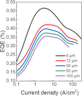
Figure 2: EQE of InGaN/GaN MQW red micro-LEDs with different device sizes.
The peak external quantum efficiency (EQE) ranged from 0.52% for the 5μm LED down to 0.36% for 100μm (Figure 2). The injections at which the peak occurred varied between 3A/cm2 and 5A/cm2, but without any clear trend, suggesting that the differences were due to process variations. By contrast, the competing red LED technology based on III-phosphide materials suffers a large shift in peak EQE injection current with size.
The higher EQE for the smaller InGaN devices is explained as being due both to the reduction of sidewall recombination, relative to phosphide-based LEDs, and higher light-extraction efficiency (LEE).
The carriers in InGaN are more likely to be trapped in localized states, rather than traveling to the sidewalls for non-radiative recombination. The small devices also allow more light to escape rather than being trapped by total internal reflection effects, increasing LEE.
The team also compares their work with recent reports from University of California at Santa Barbara (UCSB) and South China Normal University for red InGaN micro-LEDs on silicon. The USCB and South China data points for peak EQE were 0.021% and 2.3%, respectively.
The team sees the 5μm device as being particularly suitable for displays: the peak EQE occurs around 3A/cm2, which corresponds to a low drive current of 0.75μA, which could be supplied by mainstream silicon CMOS device drivers.
The researchers suggest that further developments could enhance the EQE such as by removing the silicon substrate through wafer bonding, by optimizing the device structure for higher LEE, and by optimizing the buffer to alleviate strain induced by high indium incorporation.
The team also demonstrate the ability to produce images by selective wiring on 5μm and 12μm LED arrays (Figure 3). The smaller devices naturally achieved a higher resolution.
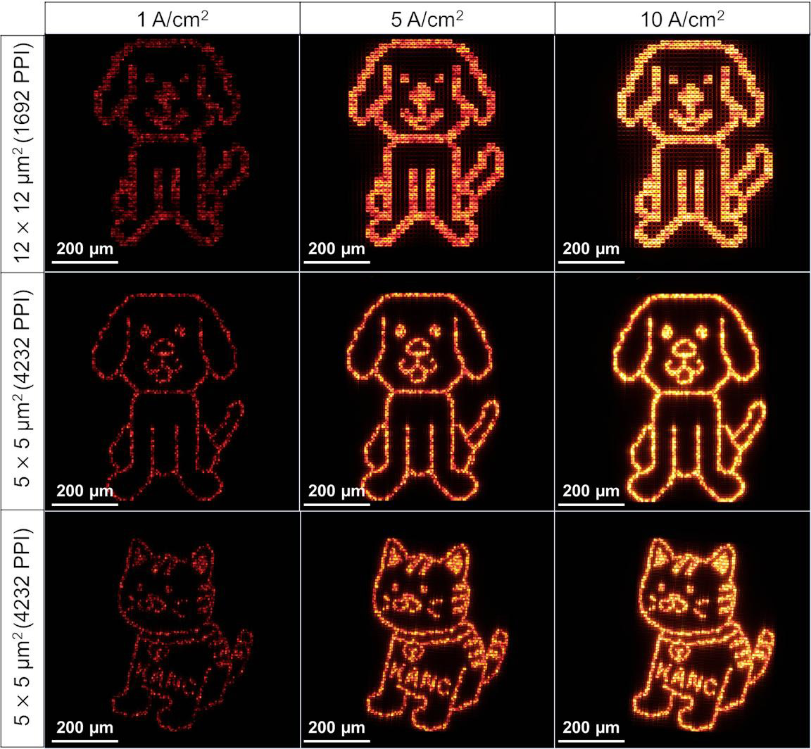
Figure 3: Images of various arrays being driven at various injections.
Given the limitations of InGaN LED devices, the researchers suggest that pulse-width modulation (PWM), rather than pulse-amplitude modulation (PAM) might be a better method to control LED brightness. The said limitations include efficiency and wavelength variations with current injection, hence the desirability of using a fixed current injection amplitude.
The researchers found a linear dependence of light luminance between 476nits and 4148nits (candela/m2) for pulse duty cycles varying between 10% and 90%, respectively, on a 12μm LED biased at 3.3V, giving current injection of 3A/cm2.
The researchers comment: “These measurements confirmed that it is possible to represent grayscale with red emission without peak shift using PWM in InGaN/GaN red micro-LED devices.”
InGaN micro-LEDs GaN InGaN MOCVD
https://doi.org/10.1364/OE.525680
The author Mike Cooke is a freelance technology journalist who has worked in the semiconductor and advanced technology sectors since 1997.


