


News: Microelectronics
4 July 2024
Magnesium intercalation in gallium nitride
Researchers based in Japan report on their studies of magnesium (Mg)-intercalated gallium nitride (GaN) superlattices (MiGs), using a spontaneous process [Jia Wang at al, Nature, published online 5 June 2024].
The team included researchers from Nagoya University, Meijo University, and Osaka University. Work at Nagoya and elsewhere has previously been reported on GaN p–n junction and p-type GaN Schottky barrier diodes, which use the MiGs structure to enhance performance.
The researchers comment: “In our electrical characterizations, we demonstrate that incorporating the MiGs structure modifies the surface potential of GaN. This provides considerable technological advantages, enhancing the barrier height of n-type Schottky barrier diodes on undoped GaN and enabling the otherwise difficult realization of ohmic contact on p-type GaN.”
Mg is the most common means to create p-type conductivity (hole transport) in GaN, where the Mg atoms grab electrons from the valence band, leaving relatively mobile holes. The researchers see this as a zero-dimensional (0D) effect, in contrast to their 2D MiGs structures.
The team comments: “The origin of ionized acceptors in the MiGs structure is probably induced by the polarization field owing to the periodic polarity transition in GaN, rather than interstitial Mg, which is electrically inactive.”
The researchers suggest that the MiGs phenomenon could also be used to increase Schottky barrier heights for improved Schottky diode performance.
Another aspect may be enhanced temperature management, although this would depend on the results of future characterization work, in particular the improved thermal transport the record-high compressive strain achieved in the c-direction.
The team also comments: “Analogous to strained silicon, applying strain to modify the band structure of GaN has been identified as a strategy to enhance carrier mobility. However, achieving and maintaining high elastic strain in GaN to demonstrate this enhancement has been difficult.”
![Figure 1: a-c. Cross-sectional high-angle annular dark-field scanning transmission electron microscopy (HAADF-STEM), progressively magnified, of 2D-MiGs. Dark lines indicate monoatomic 2D-Mgi sheets perpendicular to c-axis (the [0001] direction). d. Integrated differential phase contrast (iDPC)-STEM image (red box in c, magnified). e. Schematic of MiGs structure from d, detailing positions of constituent atoms. f. Atomically resolved energy-dispersive x-ray (EDS) spectra across localized portion of superlattice. HAADF-STEM image (top) with arrow shows line-scanning direction. g. Atomically resolved EDS elemental maps for Ga, N and Mg in same region as f. Scale bars: 10nm (a); 2nm (b); 1nm (c); 500pm (f, top); 500pm (g).](24071_nagoya_f1.jpg)
Figure 1: a-c. Cross-sectional high-angle annular dark-field scanning transmission electron microscopy (HAADF-STEM), progressively magnified, of 2D-MiGs. Dark lines indicate monoatomic 2D-Mgi sheets perpendicular to c-axis (the [0001] direction). d. Integrated differential phase contrast (iDPC)-STEM image (red box in c, magnified). e. Schematic of MiGs structure from d, detailing positions of constituent atoms. f. Atomically resolved energy-dispersive x-ray (EDS) spectra across localized portion of superlattice. HAADF-STEM image (top) with arrow shows line-scanning direction. g. Atomically resolved EDS elemental maps for Ga, N and Mg in same region as f. Scale bars: 10nm (a); 2nm (b); 1nm (c); 500pm (f, top); 500pm (g).
The MiGs structure (Figure 1) was created by physical vapor deposition (electron-beam evaporation or sputtering) of 50nm Mg on single-crystalline wurtzite GaN, followed by annealing at atmospheric pressure. Lower pressure, as used in most epitaxy processes, would increase the sublimation rate of Mg, reducing the effectiveness of the intercalation effect. The Mg was not capped during the annealing. The anneal temperatures were in the range 500–800°C. The duration was typically around 10 minutes.
The researchers comment: “The rapid interstitial diffusion of Mg within GaN resulted in its segregation into single monolayer atomic sheets. These sheets then expanded in size, resembling climbing motion of edge dislocations, and aligned vertically (along the c-axis) with each other in an even and orderly manner.”
The incorporation of the MiGs domains had a non-uniform distribution, owing to the reaction’s spontaneous, diffusion-driven nature.
The researchers did not take special measures to prevent oxidation during storage of the Mg-deposited GaN before annealing (typically within a day). However, the annealing itself was carried out in an inert atmosphere of nitrogen or argon, since the temperatures involved greatly increased the potential for Mg oxidation. Photoresist patterning lift-off steps also avoided water-based processing, which quickly degraded Mg, replacing water with isopropyl alcohol (IPA).
It was found that the charge polarization of the GaN matrix swapped between Ga- and N-polar between the Mg layers.
Table 1: Summary of electrical measurement without and with MiGs: n = Hall-effect hole concentration; ρ = in-plane, van der Pauw resistivity; ρDC = THz-TDE resistivity; σDC = THz-TDE conductivity.
Sample number |
n (x1017/cm3) |
ρ (Ω-cm) |
ρDC (Ω-cm) |
σDC (S/m) |
| 1 (without MiGs) | 1.6 | 1.6 | 1.7 | 61 |
| 2 (with MiGs) | 3.0 | 1.4 | 0.26 | 380 |
| 3 (without MiGs) | 4.3 | 1.3 | 1.1 | 89 |
The researchers write: “This observation is consistent with the theoretical model, which predicts the energetically stable configuration of a monolayer of interstitial Mg segregation (2D-Mgi) onto (0001) GaN, favoring a quarter substitutional occupation of Mg in the nearest Ga layers.”
The researchers also found that the 2D-Mg sheets tend to attract each other, “similar to the attraction between two edge dislocations of opposite sign caused by the cancellation of the strain field.” They add: “This stabilizes the structure, allowing them to align vertically and expand into a larger-diameter domain, underscoring the driving force to form an ordered superlattice structure.”
One application where the MiGs structure might be useful is for creating ohmic p-contacts (Figure 2). The p-GaN was activated before deposition of the Mg by annealing to drive out hydrogen, which passivates the Mg acceptors.
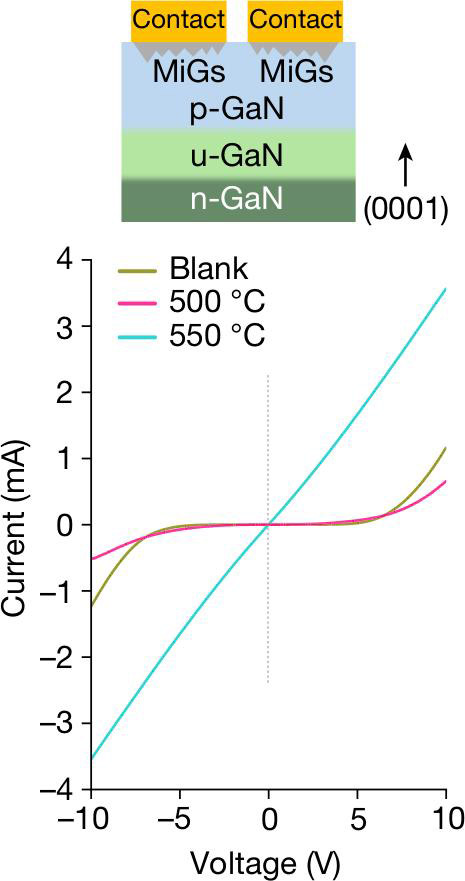
Figure 2: Current–voltage (I–V) characteristics of transfer-length-method test structures fabricated on p-type GaN samples, annealed with selective-area-patterned metallic Mg film at 500°C (10 min) and 550°C (10 min) compared with blank sample.
The researchers report: “The threshold temperature and time for the onset of MiGs formation may vary slightly depending on the initial Mg concentration in GaN. Typically, it is higher (for example, 600°C for 10 min) for unintentionally doped GaN and lower (550°C for 10 min) for GaN that is initially heavily doped with Mg.”
The team attributes the reduced contact resistivity to an increase in tunneling probability, related to a combination of factors that could include increased acceptor concentrations and decreased effective hole masses.
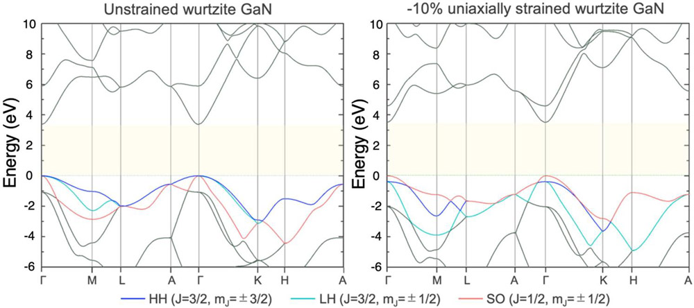
Figure 3: Calculated electronic band structures of unstrained wurtzite GaN (left) and −10% compressively-strained wurtzite GaN (right).
The smaller hole mass is related to an expected raising of the ‘split-off’ (SO) band, relative to the light hole (LH) and heavy hole (HH) bands due to the compressive strain found in the MiGs structure (Figure 3), of the order −10% out-of-plane, according to HAADF-STEM strain mapping. The ‘A’ direction of the band structure represents carrier motion in the vertical ‘c’ growth direction of the wurtzite GaN. The SO band has lighter holes, particular when traveling along the Γ (the symmetry point) to A direction, enabling increased mobility under electric field/potential biases.
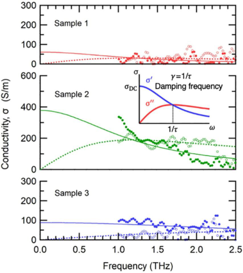
Figure 4: Real (σ′) and imaginary (σ″) parts of the conductivity, according to terahertz time-domain ellipsometry (THz-TDE). Inset: Drude model expectation used to determine DC conductivity. Samples 1 and 3 represent light-doped and heavily-doped p-GaN without MiGs. Sample 2 used the same material as 1, but with added MiGs regions.
The team used THz-TDE to assess the conductivity (Figure 4). Unlike the more usual van der Pauw measurements, THz-TDE allows assessment of vertical conductivity in the c-direction. van der Pauw structures measure only in-plane conduction (Table e). In particular, while the van der Pauw resistivities were similar for all three samples, the THz-TDE showed p-GaN with MiGs having more than 4x enhanced conductivity.
The author Mike Cooke is a freelance technology journalist who has worked in the semiconductor and advanced technology sectors since 1997.


