


News: Microelectronics
17 June 2024
Fraunhofer IAF presents 1200V GaN HEMTs at PCIM Europe
At Power, Control and Intelligent Motion (PCIM) Europe 2024 in Nuremberg (11–13 June), Fraunhofer Institute for Applied Solid State Physics (IAF) of Freiburg, Germany presented the current state of its development of novel technologies for lateral and vertical gallium nitride (GaN) transistors with blocking voltages above 1200V.
The Institute is currently working on realizing GaN-based HEMT technologies with blocking voltages up to and above 1200V, which can be used for numerous CO2 reduction measures as part of the energy transition, such as bidirectional charging of electric vehicles. GaN HEMTs are intended to provide an alternative to already available silicon carbide (SiC) metal-oxide semiconductor field-effect transistors (MOSFETs), which are very cost-intensive and therefore not suitable for widespread use. Fraunhofer IAF is pursuing several approaches for this purpose: the processing of GaN HEMTs on silicon substrates (GaN-on-Si HEMTs), the use of highly insulating carrier substrates such as sapphire, SiC or also GaN (GaN-on-insulator HEMTs) and the development of vertical GaN technologies.
GaN-on-Si HEMTs, GaN-on-insulator HEMTs and vertical GaN HEMTs for high-voltage applications
All approaches enable high-performance, efficient and cost-effective high-voltage GaN components with great application potential in key technological areas of the energy transition.
Lateral GaN-on-Si HEMTs are already commercially available, but are limited to a blocking voltage of 650V due to limited GaN layer thicknesses. By continuously optimizing the material and its processing (epitaxy, processing, structuring), researchers at Fraunhofer IAF have been able to demonstrate GaN-on-Si HEMTs with static blocking voltages of over 1200V. In addition, the power components were switched up to 1100V in an application-oriented measuring stand (double-pulse measurements).
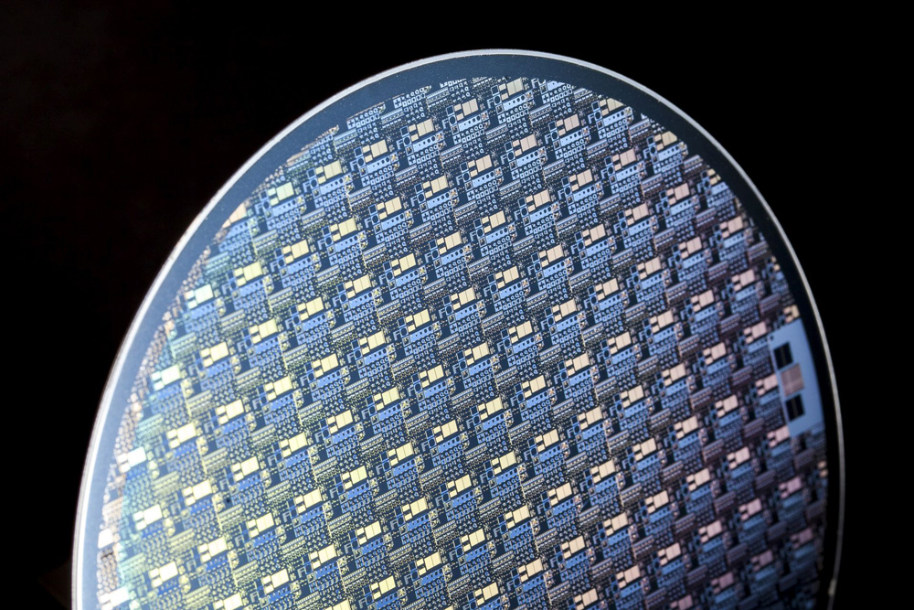
Picture: GaN-on-Si wafer comprising vertical components, developed by Fraunhofer IAF, © Fraunhofer IAF.
In the second approach, the researchers replace the conductive silicon with highly insulating carrier substrates such as sapphire, SiC or GaN, which virtually eliminates the voltage limit.
Lateral GaN-on-sapphire HEMTs can be manufactured cost-effectively based on relevant preliminary work for light-emitting diode applications and can be produced in existing production lines.
Vertical GaN technologies, in which the current flow runs vertically through the material layers, enable even greater performance with higher efficiency and integration capability at the same time. Within the next decade, the researchers at Fraunhofer IAF want to make vertical GaN power ICs suitable for industrial use. The aim is also to help to shape the next technological leap in the transformation towards a climate-neutral society.
More about 1200V GaN HEMTs at PCIM Europe
At PCIM Europe, Dr Richard Reiner provided an overview of the development of lateral and vertical GaN power ICs in his presentation ‘Lateral and Vertical GaN Power ICs: Status and Future’.
In the ‘Device Concepts’ session, Reiner provided an insight into the various lateral 1200V GaN technologies in his presentation ‘More than 1200V Breakdown and Low Area-Specific On-State Resistances by Progress in Lateral GaN-on-Si and GaN-on-Insulator Technologies’.
Also, in the session ‘GaN Converters’, Fraunhofer IAF’s Dr Stefan Mönch gave a presentation ‘Over 99.7% Efficient GaN-Based 6-Level Capacitive-Load Power Converter’.


