


News: Microelectronics
27 June 2024
Nexperia investing $200m in Hamburg site to add wide-bandgap semiconductors
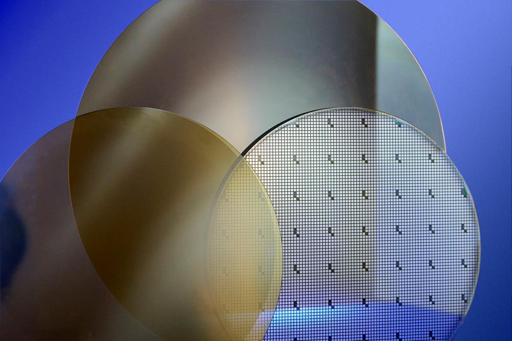
Discrete device designer and manufacturer Nexperia B.V. of Nijmegen, The Netherlands (a subsidiary of Wingtech Technology Co Ltd) plans to invest $200m (€184m) to develop wide-bandgap semiconductors (WBG) such as silicon carbide (SiC) and gallium nitride (GaN), and to establish production infrastructure at its site in Hamburg-Lokstedt, Germany. At the same time, wafer fab capacity for silicon (Si) diodes and transistors will be increased. The investments were jointly announced with Hamburg’s Minister for Economic Affairs Dr Melanie Leonhard on the occasion of the 100-year anniversary of the production site.
To meet the growing long-term demand for efficient power semiconductors, all three technologies (SiC, GaN, and Si) will be developed and produced in Germany, starting from June.
“This investment strengthens our position as a leading supplier of energy-efficient semiconductors and enables us to utilize available electrical energy more responsibly,” says Achim Kempe, chief operating officer & managing director at Nexperia Germany. “In the future, our Hamburg fab will cover the complete range of WBG semiconductors while still being the largest factory for small-signal diodes and transistors. We remain committed to our strategy of producing high-quality, cost-efficient semiconductors for standard applications and power-intensive applications, while addressing one of the greatest challenges of our generation: meeting the growing demand for energy and while reducing the environmental footprint.”
The first production lines for high-voltage GaN D-mode transistors and SiC diodes started up in June. The next milestone will be cost-efficient 200mm production lines for SiC MOSFETs and GaN HEMTs, established at the Hamburg factory over the next two years.
At the same time, the investment will help to further automate the existing infrastructure at the Hamburg site and expand silicon production capacity by systematically converting to 200mm wafers. Following expansion of the cleanroom areas, new R&D laboratories are being built to ensure a seamless transition from research to production in the future.
In addition to advancing technology, Nexperia expects the initiative to stimulate local economic development, helping to secure and create jobs, while enhancing the European Union’s semiconductor self-sufficiency. Nexperia says that it works closely with universities and research institutes to benefit from each other’s expertise and promote highly qualified employee training, relying on a robust R&D ecosystem in Hamburg and throughout Europe. Development partnerships and co-operations — e.g. in GaN technology as part of the Industrial Affiliation Program (IIAP) of the nanoelectronics research center imec in Leuven, Belgium — play a crucial role.
“The planned investment enables us to bring WBG chip design and production to Hamburg. However, SiC and GaN are by no means new territory for Nexperia. GaN FETs have been part of our portfolio since 2019, and in 2023 we expanded our range of products to include SiC diodes and SiC MOSFETs, the latter in collaboration with Mitsubishi Electric,” says Stefan Tilger, chief financial officer & managing director at Nexperia Germany. “Nexperia is one of the few suppliers to offer a comprehensive range of semiconductor technologies, including Si, SiC and GaN in both E-mode and D-mode. This means we offer our customers a one-stop shop for all their semiconductor needs.”
Vishay completes acquisition of Nexperia’s Newport Wafer Fab following UK Government approval
Mitsubishi Electric and Nexperia to co-develop SiC power semiconductors
Nexperia expands wide-bandgap range by entering high-power silicon carbide diode market


