


News: Microelectronics
20 June 2024
GaN HEMTs on 8-inch sapphire
Xidian University and Guangdong Ziener Technology Company Ltd in China claim the first fabrication of gallium nitride (GaN) high-electron-mobility transistors (HEMTs) on 8-inch sapphire substrates [Junbo Wang et al, IEEE Transactions on Electron Devices, published online 30 May 2024]. The OFF-state breakdown voltages reached beyond 1200V.
The researchers hope that their work will enable sapphire to commercially compete with GaN HEMT devices on large-diameter silicon (8- and 12-inch Si). Previously, GaN HEMTs/sapphire have been produced on 6-inch diameter substrates, increasing cost per unit.
The use of sapphire substrates enables thinner GaN buffers, and simpler epitaxy structures, due to the higher-quality growth, relative to material grown on silicon. The sapphire substrate is also more electrically insulating than silicon, which should enable kiloVolt blocking capability. [Sapphire is also more thermally insulating, which could hamper the heat dissipation needed for high power densities.]
GaN HEMTs with less than 650V ratings have seen deployment in fast chargers, class D-Audio amplifier, power tools, and home appliances. Going beyond 650V, GaN HEMTs/sapphire could open the way to industrial applications such as motor drivers and charging piles.
The researchers performed metal-organic chemical vapor deposition of III-nitride epitaxial material on 1.15mm-thick, 8-inch diameter sapphire substrates (Figure 1). The layer growth sequence was: 35nm aluminium gallium nitride (AlGaN) nucleation, 1.98μm GaN buffer, 420nm GaN channel, 1nm AlN spacer, 21nm Al0.27Ga0.73N barrier, and, 2nm in-situ silicon nitride (SiN) cap.
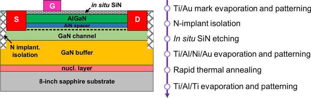
Figure 1: Cross-sectional schematic of fabricated GaN HEMTs on 8-inch sapphire and processing flow.
HEMTs were fabricated with ohmic titanium/aluminium/nickel/gold (Ti/Al/Ni/Au) source/drain (S/D) metal stacks. The gate (G) metal was Ti/Al/Ti. Electrical isolation was provided by nitrogen-ion implantation.
Sheet resistance mapping showed a wafer-level non-uniformity of 4%. The average resistance was 310Ω/square. The warpage of the GaN/sapphire was 30μm.
The ω rocking curves for x-ray diffraction from the (002) and (102) planes demonstrate full-width at half maximum (FWHM) values of 588 arcsec and 1032 arcsec, respectively.
The researchers comment: “Further improvement of the epitaxy uniformity and quality can be made by tuning the buffer stack, gas flow, chamber pressure, temperature field, and so on.”
The fabricated HEMTs aimed at 200V ratings. The gate length was 4μm, while the gate–source (GS) and gate–drain (GD) distances were 1.5μm and 6μm, respectively. The gate width was 100μm.
The device operated in ‘normally-on’ depletion mode with a negative threshold voltage of −4.2V. The specific on-resistance (RON) was 6.5Ω-mm. The RON was higher in devices near the center of the wafer, reaching 8.6Ω-mm. The team says that this was the result an “intrinsic problem” of the MOCVD chamber, along with a variation of contact resistance in the range 0.7–1.5Ω-mm.
The OFF-state breakdown of the HEMT devices with 6μm GD distance occurred at more than 500V, meeting the requirements of 200V ratings. Extending the GD distance to 16μm increased the breakdown beyond 1200V, meeting 650V requirements. The researchers believe that field plates and passivation improvements could boost performance further.
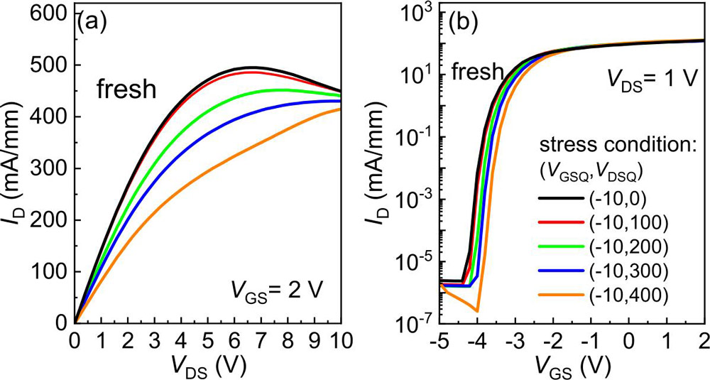
Figure 2: (a) Drain current–voltage (ID–VD) and (b) ID–gate voltage (VG) curves of the 200V GaN HEMTs on sapphire with 6μm GD distance after various OFF-state stresses.
Under 400V stress the 200V HEMTs suffered a current collapse of 41% (Figure 2). For 200V stress, the collapse was reduced to 15%. The researchers see the collapse as being due to a combination of a threshold shift and charge trapping effects. Again, field plate structures could alleviate collapse/dynamic RON impacts, the team suggests.
GaN HEMTs GaN Sapphire substrates
The author Mike Cooke is a freelance technology journalist who has worked in the semiconductor and advanced technology sectors since 1997.


