


News: Microelectronics
3 May 2024
ETRI develops 3kV-class gallium oxide epilayer and device technologies
Supported by South Korea’s Ministry of Culture, Sports and Tourism, and in collaboration with the Korea Institute of Ceramic Engineering and Technology (KICET), South Korea’s non-profit, government-funded Electronics and Telecommunications Research Institute (ETRI) has developed core material and device process technologies for gallium oxide ( Ga2O3) power semiconductors, namely the first 3kV-class gallium oxide power semiconductor metal-oxide-semiconductor field-effect transistor (MOSFET) device developed in Korea.
Gallium oxide has been actively researched worldwide as a key material for next-generation power semiconductors. Japan and the USA have held technological superiority in this field, but ETRI reckons that its development has narrowed the gap.
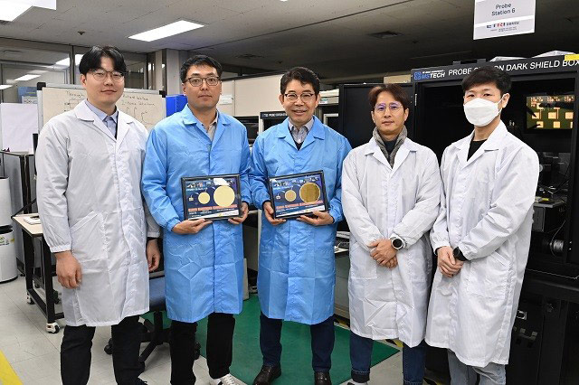
Picture: Dr Mun Jae-kyoung’s research team.
The 3kV class is applicable to urban rail, subways and ultra-fast electric vehicle chargers. By incorporating gallium oxide 3kV-class power semiconductors into ultra-fast electric vehicle chargers, it is possible to significantly reduce charging times from the 30-minute range to less than 20 minutes.
As they are essential components used across national industries (including mobile and quantum communications, electric vehicles, solar and wind power generation, power transmission, defense, aerospace, and quantum computing), power semiconductor devices comprise one of South Korea’s 12 national strategic technologies related to materials, components and equipment. However, currently more than 95% depend on imports from abroad. Localization of next-generation gallium oxide power semiconductor materials and device technologies therefore holds significant importance from the perspective of South Korea achieving self-reliance in national strategic technologies.
The gallium oxide epitaxial layer technology developed by the research team involves a process of growing multiple layers of high-quality conductive thin films on a single-crystal substrate.
Dr Jeon Dae-woo’s research team at KICET has localized the high-quality beta- Ga2O3 epitaxial growth technology using metal-organic chemical vapor deposition (MOCVD), which is expected to be used globally for mass production of large-diameter epitaxial wafers. As well as enabling the growth of epitaxial layers with thicknesses ranging from nanometers to microns, this technology also allows a wide range of adjustment in electron concentration. Consequently, this facilitates the development of power semiconductor devices with various voltage and current capabilities, bringing it closer to mass-production technologies.
Furthermore, the gallium oxide device process technology developed by the team presents a wafer-scale integration process technology for fabricating large-size power semiconductor devices. This technology encompasses the formation of micro-patterns on the epilayers of Ga2O3 substrate, low-damage etching, deposition, and thermal processing.
Dr Mun Jae-kyoung’s research team at ETRI has developed a superior performance 3kV-class MOSFET device using the epilayers directly developed by the KICET research team, rather than commercial epilayers on single-crystal wafer imported from Japan.
In particular, a new epitaxial structure capable of reducing leakage current to the level of picoamperes (pA) was developed. Furthermore, the achievement includes the development of new device and process technologies that significantly enhance the breakdown voltage to exceed 3kV.
The localization of gallium oxide power semiconductor technology is given paramount importance for enhancing next-generation global competitiveness and preempting new markets, especially in a context where most wide-bandgap (WBG) power semiconductor technologies, such as gallium nitride (GaN) and silicon carbide (SiC), currently rely on overseas sources.
The research team states that the development of gallium oxide epilayers and power semiconductor MOSFET technologies can cut manufacturing costs to one-third to one-fifth compared with existing power semiconductors. This cost reduction through localization enables South Korea to take a leading position in the high-value-added industry of next-generation power semiconductors, the team reckons.
Moreover, gallium oxide semiconductors exhibit superior material properties, enabling them to withstand higher voltages. This not only allows a reduction in the size of power semiconductor devices by 50% or more, facilitating miniaturization, but also improves power conversion efficiency. Consequently, the performance of power semiconductor devices can be enhanced by more than tenfold, increasing the price competitiveness of these devices more than 20-fold compared with existing power semiconductors.
The research team explained that gallium oxide power semiconductor devices could not only enhance power conversion efficiency but also significantly reduce the size of inverter and converter systems to less than one-tenth of their existing dimensions.
It is anticipated that applying these devices to high-power industries, such as power transmission and distribution networks, high-speed railways, data centers, quantum computers, and electric vehicles, will substantially boost energy-saving effects.
Focus on commercializing 4-inch Ga2O3 power MOSFET process using plating process
ETRI is currently focusing on the world’s first development and commercialization of a 4-inch gallium oxide power semiconductor MOSFET device process using a plating process with a thickness of 4µm. Thus, it is expected that the acquisition of mass-production technology for gallium oxide power semiconductors, utilizing domestically developed 4-inch large-area epitaxial materials and device process technologies, will also be possible in near future.
According to a 2023 report by Japan’s Yano Research Institute, the global power semiconductor market will grow to about KRW49 trillion by 2030, with the gallium oxide market reaching KRW1.7 trillion.
“The localization of gallium oxide epitaxial wafers, which are key components of next-generation power semiconductors, will enable a reduction in the epitaxial wafer cost, which are over 40% of the manufacturing costs of domestic power semiconductors and achieve material independence,” says Dr Jeon Dae-woo, a senior researcher at KICET.
“We anticipate the timing for the integration of gallium oxide power semiconductors into systems to be further accelerated,” says Dr Mun Jae-kyoung, the project general manager at ETRI. “We plan to be the first in the world to commercialize kilovolt-class gallium oxide power semiconductor MOSFET devices.”


