


News: Microelectronics
9 May 2024
Poly- MoS2 FETs integrated on 200mm substrate
Samsung Advanced Institute of Technology (SAIT) and Seoul National University in South Korea, and Massachusetts Institute of Technology in the USA, have reported 200mm-wafer-scale integration of polycrystalline molybdenum disulfide ( MoS2) transistors [Kwon, Junyoung et al, Nature Electronics, published online 24 April 2024].
MoS2, a transition-metal dichalcogenide (TMD) material, consists of layers held together with relatively weak van der Waals forces. Current flows in such materials are confined to two-dimensional planes. The researchers comment: “Two-dimensional semiconductors are an attractive material for making thin-film transistors due to their scalability, transferability, atomic thickness and relatively high carrier mobility. There is, however, a gap in performance between single-device demonstrations, which typically use single-crystalline two-dimensional films, and devices that can be integrated on a large scale using industrial methods.”
The team redesigned the process for creating MoS2 FETs to enable use of polycrystalline materials to achieve comparable performance to single-crystal devices created on small flakes of material under laboratory conditions. In particular, the contact resistance of the source/drain contacts was reduced by using pre-patterned bottom contacts, rather than the more usual contacts deposited on top.
The researchers comment: “These capabilities are attributed to suppressing metal-induced gap states (MIGS) and pinning the Fermi level near the conduction band, thereby reducing the Schottky barrier to zero and reducing the contact resistance.”
Devices based on 2D TMD structures could be deployed at thin-film transistors (TFTs) for consumer electronic and optoelectronic products. TFTs are key components of display backplanes, and the scaling potential of 2D TMD structures would enable higher resolutions. SAIT et al see poly-TMD transistors as having better prospects than other technologies such as amorphous and polycrystalline silicon, oxide and organic semiconductors, and carbon nanotubes (CNTs). The thickness of devices being on the atomic scale raises prospects for flexible, wearable and conformable electronics.
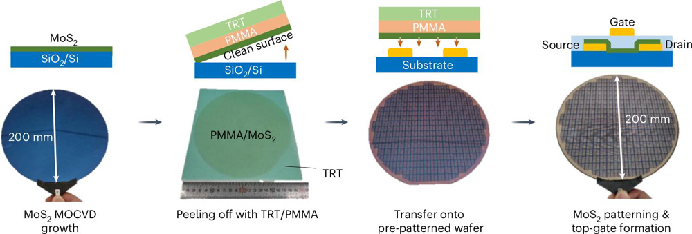
Figure 1: Simplified 200mm-wafer-scale fabrication process for bottom-contact FET.
The fabrication began with metal-organic chemical vapor deposition (MOCVD) of monolayer MoS2 on a 200mm-diameter silicon dioxide on silicon (SiO2/Si) substrate (Figure 1). The SiO2 layer was 100nm thick.
The researchers used a high-throughput, cold-wall, showerhead MOCVD system. The precursors were molybdenum hexacarbonyl (Mo(CO)6) and diethyl disulfide ((C2H5)2S2). The growth process took place at 800°C at 5Torr. The growth time was 12 minutes, consisting of five cycles of precursor co-injection and purging.
The MoS2 layer was peeled off the growth substrate using poly(methyl methacrylate) (PMMA) and thermal release tape (TRT).
The researchers comment: “The low adhesion energy between the as-grown MoS2 and SiO2 originates from the residual strain and the use of an automatic transfer machine substrate, as well as additional strain that arises from PMMA curing, enabling a 100% exfoliation yield.”
The MoS2 layer was transferred onto the 200mm silicon host substrate. The researchers took particular care to maintain clean surfaces of both the MoS2 and Au to ensure uniform, high-yield performance of the fabricated devices.
The host substrate was prepared with atomic layer deposition (ALD) hafnium dioxide ( HfO2) etch stop layer and pre-patterned titanium/gold (Ti/Au) source/drain contacts. The team comments: “ HfO2 was chosen because it provides stronger adhesion to MoS2 than other oxides.”
The height of the metal contacts was critical — higher contacts resulted in lower mobility and yields. The contacts used finally were 30nm high. Further, sulfur and gold form tight bonds, preventing peeling of the monolayer during further processing.
The top gate stack consisted of 20nm aluminium oxide (Al2O3) or 10nm HfO2 dielectric with 30nm Au electrode. The dielectrics were applied by ALD.
The fabrication, apart from the semi-automatic layer transfer, was performed at SAIT’s 200mm facility.
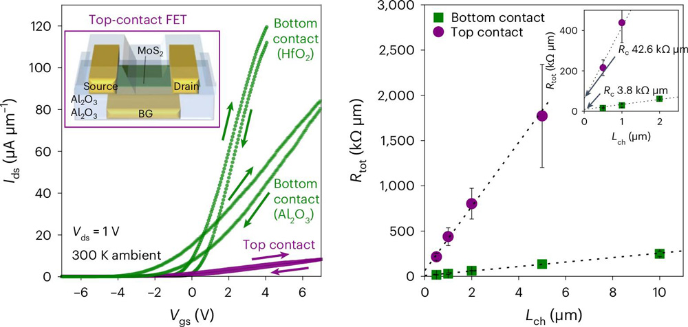
Figure 2: Left: Linear-scale transfer curves (Ids–Vgs) for 500nm-channel-length transistors with the source/drain contacts on the bottom or top. Inset: Top-contact FET schematic. Right: Specific contact resistances extracted using transfer length method.
The researchers compared the performance of their bottom-contact devices with reference FETs with the structure inverted resulting in a top-contact (Figure 2). The team comments: “When comparing devices with the same Al2O3 dielectric, bottom-contact FETs consistently exhibit performance approximately one order of magnitude higher than top-contact FETs.”
The 1V-bias on-current of the bottom-contact devices reached 84μA/μm and the field-effect mobility (μFE) was 18cm2/V-s. With the high-k HfO2 dielectric, these values reached 120μA/μm and 21cm2/V-s, respectively.
The researchers comment: “The device performance in terms of field-effect mobility and ON-current of the bottom-contact FET based on poly- MoS2 is on par with that of a conventional top-contact device with single-crystal MoS2. Therefore, good contact engineering can help to overcome differences in the qualities of channel materials.”
The team also reports a 99.97% yield on the basis of only one device failure out of 2,976 on a 200mm wafer.


