


News: LEDs
22 May 2024
Reversing size effects in cyan-green micro-LEDs
Researchers based in China report progress in eliminating size effects in micron-scale cyan-green light-emitting diodes (LEDs) [Peng Zhang et al, ACS Photonics, v11, p2045, 2024]. In fact, the smaller 10µm devices fabricated by the team from the Suzhou Institute of Nano-Tech and Nano-Bionics (SINANO) and the University of Science and Technology of China showed higher efficiency than larger devices (15µm and 20µm).
Size effects in micro-LEDs are usually the result of non-radiative sidewall recombination, which becomes increasingly significant as devices shrink. The researchers used a wet chemical treatment on the sidewalls oriented to the ‘M’ planes of the gallium nitride (GaN) hexagonal crystal structure. The chemical etch preferentially smoothed the surfaces to pure M planes, from the rough alignment provided by a previous plasma etch.
In theory, devices with M-plane sidewalls could be arranged as arrays of triangles, but hexagons should provide much better current-spreading performance. The researchers see micro-LEDs as driving future display developments, particularly for augmented reality and virtual reality applications.
The epitaxial structure for the LEDs was grown by plasma-assisted molecular beam epitaxy on 2µm-thick GaN-on-sapphire templates prepared by metal-organic chemical vapor deposition. The active region consisted of multiple layers (5x) of self-assembled indium gallium nitride (InGaN) quantum dots (MQDs) in GaN. The dot layers were 3nm spaced by 11nm GaN barriers. The structure also included a 13nm aluminium gallium nitride (AlGaN) electron-blocking layer (EBL) between the active region and the hole-injecting 150nm top p-GaN layer. The electron-injection layer was 630n n-GaN between the template and active region.
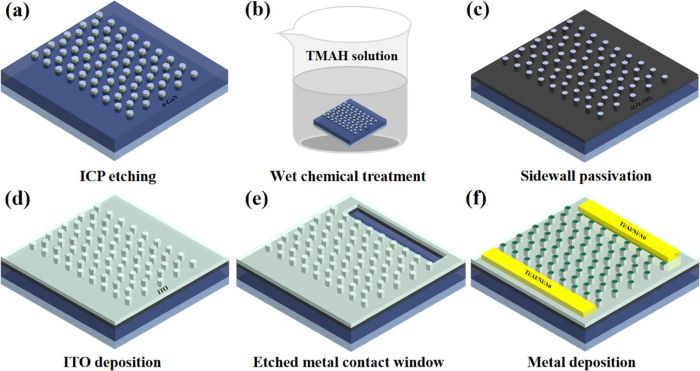
Figure 1: Process flow of cyan-green GaN-based QD micro-LED array: (a) ICP etching, (b) wet chemical treatment, (c) sidewall passivation, (d) ITO deposition, (e) etched metal contact window, and (f) metal deposition.
The epitaxial material was etched into hexagonal micro LEDs in two steps (Figure 1): using inductively coupled plasma (ICP) to a depth of 550nm, followed by wet chemical treatment with tetramethylammonium hydroxide (TMAH) solution at 85°C for 2 hours to remove sidewall defects and etch damage (Figure 2). The etching produced arrays of 77 hexagonal micro-LEDs with the sides aligned with the M-plane family ({10-10}) of the hexagonal wurtzite GaN crystal structure. The TMAH treatment transformed the sidewalls from a roughly 45° bevel angle to near vertical, along with reducing the surface roughness and, presumably, defects.
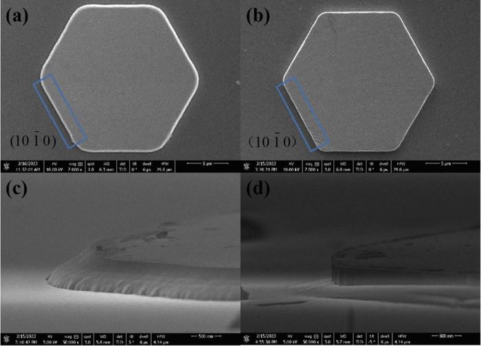
Figure 2: Scanning electron microscope (SEM) images of 10µm hexagonal QD LED. Top views (a) before and (b) after TMAH treatment. Bird’s-eye views of the sidewall before (c) and after (d) treatment.
The sidewall passivation consisted of 20nm atomic layer deposition aluminium oxide (Al2O3) and 200nm plasma-enhanced chemical vapor deposition silicon dioxide (SiO2).
The p-contact electrode was 130nm indium tin oxide (ITO). After etching down to the n-GaN layer, titanium/aluminium/nickel/gold metal contacts were applied to the p- and n-sides of the device.
The power density and efficiency dependence went against the usual expectation of reduced performance of the smaller devices due to surface-related non-radiative recombination (Figure 3). In fact, the smaller 10µm-side devices achieved a higher light output power density, and higher efficiency than the larger 15µm and 20µm LEDs.
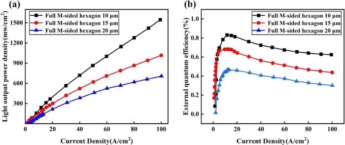
Figure 3: (a) Light output power (LOP) density and (b) external quantum efficiency (EQE) versus current density for different-sized micro-LED arrays.
The researchers suggest that the increased performance was a combination of the TMAH treatment effectively tackling the size effect in terms of surface repair, and the smaller size allowing better current spreading and higher light extraction efficiency (LEE) to be realized.
The peak EQEs were 0.47%, 0.68% and 0.83% for the 20µm, 15µm and 10µm devices, respectively. Also, the peaks occurred around the same injection current density. The researchers comment: “The peak EQE of conventional micro-LEDs tends to shift toward higher current densities due to non-radiative recombination caused by sidewall defects.” The team suggests that this indicates that the rate of non-radiative recombination is not increased in the smaller micro-LED array.
The low EQE compared with conventional quantum well (QW) devices was attributed to at least two factors:
1. Low-temperature growth of the GaN quantum barrier layer. The low temperature results in lower-quality material, but is used to avoid damage of the underlying InGaN QD layers: indium tends to desorb at higher temperatures.
2. Low electron capture cross-section of QDs versus QWs. This could be improved by increasing the area density of QDs, it is hoped.
The emission wavelength of the devices at low current density (1A/cm2) was around 503nm. When the injection reached 100A/cm2, the wavelengths had blue-shifted by 12nm, 7.7nm and 7.6nm for the 10µm, 15µm and 20µm LED arrays, respectively.
https://doi.org/10.1021/acsphotonics.4c00211
The author Mike Cooke is a freelance technology journalist who has worked in the semiconductor and advanced technology sectors since 1997.


