


News: Optoelectronics
2 May 2024
PCSEL emits at more than 300mW CW at 1550nm wavelength
Sumitomo Electric Industries Ltd and Kyoto University in Japan have claimed a record continuous wave (CW) output power exceeding 300mW for a 1550nm-wavelength photonic-crystal surface-emitting laser (PCSEL) on an indium phosphide (InP) platform [Takeshi Aoki et al Appl. Phys. Express, p17, p042004, 2024].
The researchers note: “While single-mode lasing at a peak output power of up to 100mW under pulsed conditions has been reported using 1550nm-wavelength InP-based PCSELs, CW operation of these PCSELs at output powers of hundreds of milliwatts has not been achieved, in contrast to GaAs-based and GaN-based ones.” The mentioned gallium arsenide (GaAs) and gallium nitride (GaN) PCSELs, of course, emit shorter-wavelength laser light than 1550nm.
The team sees such InP-based PCSELs as promising light sources for optical communications and LiDAR (light detection and ranging) that depend on high-power and single-mode characteristics. The 1550nm wavelength range is particularly suitable for applications where eye safety is a concern, since this wavelength is mostly absorbed in the crystalline eye lens before reaching the retina.
PCSELs use a two-dimensional (2D) photonic crystal as an optical cavity coupled to a nearby active layer. The team explains: “Lasing oscillation is achieved in the form of a broad-area 2D standing wave at a singularity point (typically Γ) in the photonic band structure.”
The PC was prepared before the epitaxy of the active layers of the laser diode by patterning and dry etching of an n-InP substrate (Figure 1). The PC structure was then encapsulated by overgrowing an InP spacer layer before the indium gallium arsenide phosphide (InGaAsP) multiple quantum well (MQW) photon-generating layer.
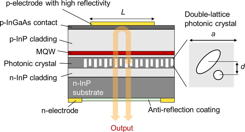
Figure 1: Schematic of 1550nm-wavelength PCSEL with double-lattice photonic crystal structure consisting of large elliptical and small circular air holes.
The researchers note: “The advantage of this fabrication process is that, by growing the active layer atop the PC layer after the dry-etching step, the risk of damaging the active layer through dry etching of the deep air holes is avoided, enabling the PC structure to be closer to the active layer.”
The laser diode was designed to have a reflective p-contact with the laser beam output emerging from a 200μm circular window on the flipped n-side of the device. The PC consisted of elliptical and circular holes in a 480nm square unit cell. The size of the cell was suitable for 1550nm-wavelength oscillations.
The device achieved 318mW peak output power at 25°C under CW operation (Figure 2). The researchers believe this is the highest reported output power for PCSELs in the 1550nm wavelength range. The wall-plug efficiency was 17.3%.
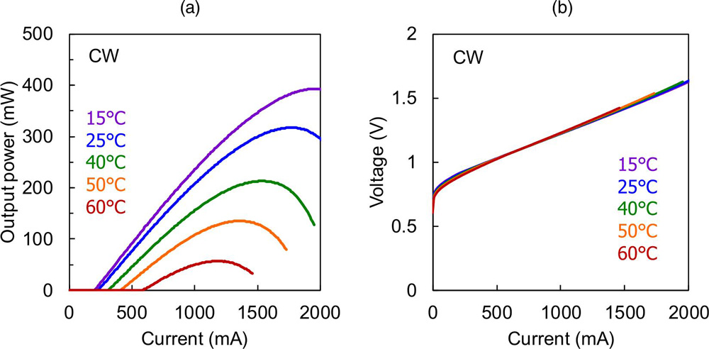
Figure 2: (a) Light output power-current (L–I) and (b) voltage–current (V–I) characteristics of fabricated 200μm-diameter PCSEL under CW conditions from 15°C to 60°C.
The Jth at 25°C (Table b) was comparable to the 0.67kA/cm2 of a 1300nm PCSEL previously reported by the researchers. The team comments: “The slight difference of Jth is attributed to larger intrinsic loss and Auger recombination at the longer wavelength.”
At 1770mA injection at 25°C, the main peak at 1546.43nm had a full-width at half maximum (FWHM) less than the 0.2nm resolution limit of the analyzer. The side-mode suppression ratio (SMSR) exceeded 60dB for currents up to 2A, and operating temperatures up to 60°C.
Table 1: CW performance characteristics at 25°C and 60°C.
Characteristic |
25°C |
60°C |
| Threshold current | 230mA | 590mA |
| Threshold current density (Jth) | 0.73kA/cm2 | 1.9kA/cm2 |
| Slope efficiency (ηSE) | 0.29W/A | 0.15W/A |
The researchers did observed a slight decrease in the SMSR with increasing current or temperature due to a small increase in intensity of emission from one of the side modes (labeled C). The divergence angle of the far-field pattern was less than 1° at 800mA, 25°C (1/e2 width).
The researchers comment: “The temperature at the center of the current injection area becomes higher than that at the periphery, resulting in the concomitant emergence of a downward-convex-shaped in-plane band-edge frequency distribution caused by a temperature-borne change of refractive index.”
https://doi.org/10.35848/1882-0786/ad3cb4
The author Mike Cooke is a freelance technology journalist who has worked in the semiconductor and advanced technology sectors since 1997.


