


News: Microelectronics
17 May 2024
Sumitomo presents pore-assisted free-standing GaN
Sumitomo Chemical Co Ltd in Japan has developed a pore-assisted separation (PAS) method for the fabrication of free-standing gallium nitride (GaN) substrates [Masafumi Yokoyama et al Appl. Phys. Express, v17, p055502, 2024].
The researchers comment: “We expect that the proposed method will open a path to realizing larger free-standing GaN substrates with good productivity.”
Sumitomo sees improved power conversion efficiency of electrical systems as being one of the key contributors to tackling the bad effects of human activity on the global climate. GaN-based devices are being developed with this end in view, since the wide-bandgap material is capable of handling larger voltages and power densities than more traditional electronic materials such as silicon.
The researchers comment: “In fact, vertical-type GaN power devices fabricated homoepitaxially on free-standing GaN substrates have exhibited superior voltage-blocking capability and low on-resistance, as expected on the basis of GaN’s nature.”
Free-standing GaN has been produced by a wide variety of methods. The key steps are growing a thick layer of GaN on a suitable substrate, such as sapphire, and then separating the GaN from the initial substrate.
Presently, Sumitomo uses a void-assisted separation (VAS) hydride vapor phase epitaxy (HVPE) growth process to produce commercial 2–4-inch free-standing GaN substrates. Sumitomo believes that its VAS method produces superior substrates. “However, if the GaN substrate size is further scaled beyond 4-inches (100mm) using the VAS method, process non-uniformities of void formation might become severe,” the researchers worry.
In particular, the VAS method has a high-temperature anneal step, which requires a higher degree of uniformity than can be realized for wafer diameters greater than 100mm. The team has thus developed a PAS method, which creates pores at room temperature.
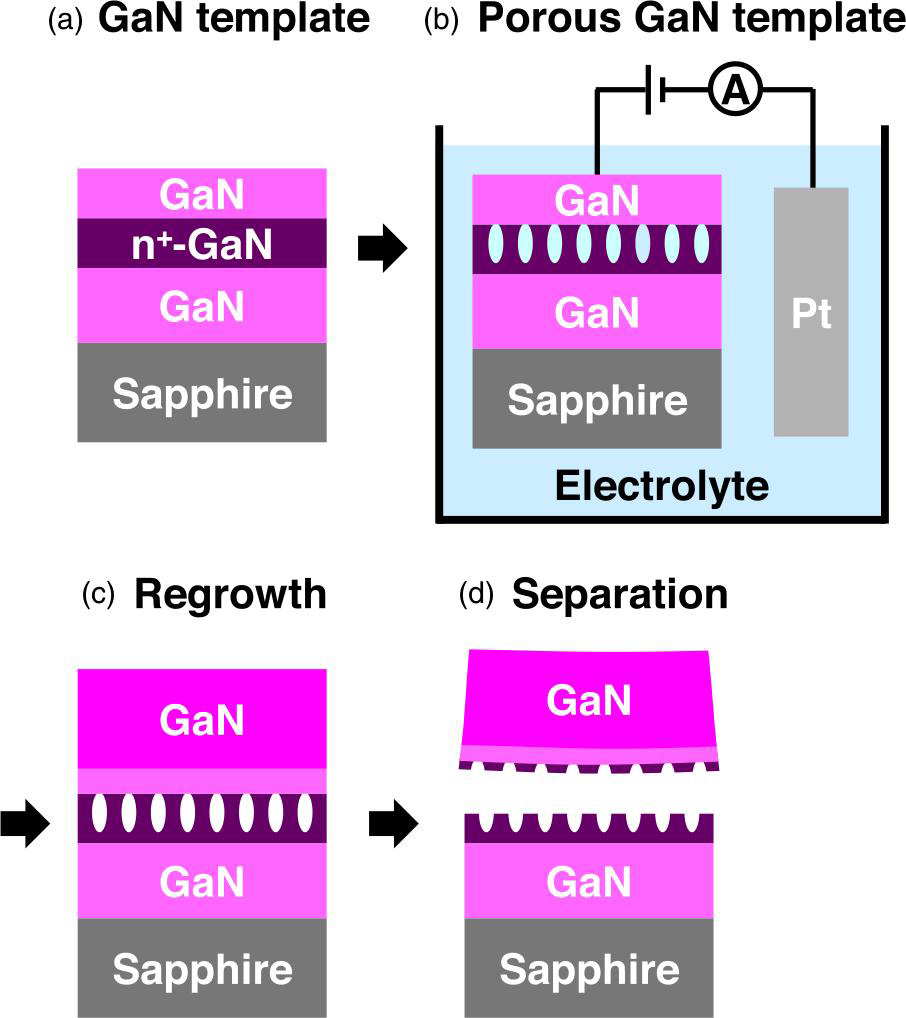
Figure 1: Process flow: (a) GaN template, (b) porosification by electrochemical etching, (c) regrowth of thick GaN layer by HVPE and (d) separation of free-standing GaN substrate from during cooling after HVPE growth.
The researchers first prepared templates for the free-standing GaN material (Figure 1), using metal-organic vapor phase epitaxy (MOVPE) or HVPE. The researchers comment: “There was no significant difference in MOVPE and HVPE GaN templates for fabrication of the porous GaN templates.”
The template consisted of an undoped base (1μm or more), heavily-doped n+-GaN (1–3μm), and lightly-doped n−-GaN layers (100–200nm). The carrier densities in the outer GaN layers were in the lower half or less than 1018/cm3 range, while the n+-GaN was in the upper half 1018/cm3 range or higher.
The middle n+-GaN layer was porosified in an electro-chemical etch process at room temperature. The electrolyte consisted of oxalic acid. The positive and negative electrodes were the thin GaN cover layer and platinum (Pt), respectively.
The team reports: “Although the as-grown GaN template before porosification showed a mirror-like surface with high transparency, the porous GaN template appeared translucent, with the mirror surface kept as it was, indicating the successful formation of a porous structure inside the GaN layer.”
The region around the positive electrode on the GaN template needed an additional etch step to porosify. The surface roughness was only increased slightly from 0.36nm to 0.45nm, according to atomic force microscopy (AFM) over a 5μmx5μm field. The height and width of the average pore could be controlled by the applied voltage.
The pore formation was explained as being due to oxidation by hole injection through Zener and/or avalanche breakdown. The researchers used applied voltages in the 10–20V range, insufficient to induce breakdown for the n−-GaN layer, but high enough to induce breakdown in dislocation cores, forming pipes to the n+-GaN for Zener and/or avalanche breakdown and pore formation in that layer.
The pores of higher-voltage electrochemical etch were larger. The variation was approximately linear between 10V and 20V with widths in the range 50–150nm, and the height in the range 50–200nm.
The materials for the free-standing GaN substrate was through HVPE regrowth at ~1000°C and atmospheric pressure. Separation of the free-standing material occurred during cooling due to the difference in thermal expansion coefficients of GaN and sapphire creating stress in the porous layer that broke the regrown material away.
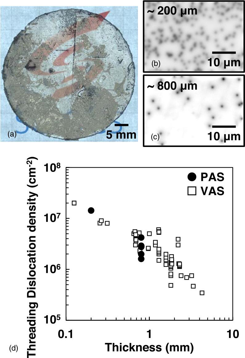
Figure 2: (a) Photograph of 800μm-thick GaN layer grown on porous GaN template. Plan-view CL images of (b) 200μm- and (c) 800μm-thick GaN grown on 20V porous GaN templates. (d) Layer thickness versus TDD values, comparing PAS and VAS separation.
HVPE growth on 20V porous material with large pores resulted in complete separation of the free-standing substrate from the template (Figure 2). The researchers report: “In contrast, the porous GaN template with small-sized pores resulted in the porous GaN template breaking as well as the sapphire substrate and without separation of the GaN layer.”
The team notes that there were Ga residues on the back-side of the free-standing wafer, showing up as gray regions on photographs. “At this initial stage of development, we were not concerned with suppressing attachment of the GaN wafer to the wafer tray during deposition of the thick GaN layer,” the researchers comment.
The threading dislocation density (TDD) for 200μm and 800μm free-standing substrates were measured by cathodoluminescence (CL) at 1.4x10⁷/cm2 and 2.7x1076/cm2, respectively. This was similar in character to the results achieved with VAS.
The researchers attempted to apply the PAS method to producing a 3-inch GaN free-standing substrate. The team were “nearly” successful in the effort “although cracks caused by crystal fixing at irregular portions remained.” The researchers hope that improvements in the HVPE wafer tray design will prevent such attachments in future work.
Free-standing GaN GaN substrates Void-assisted separation HVPE
The author Mike Cooke is a freelance technology journalist who has worked in the semiconductor and advanced technology sectors since 1997.


