News: Suppliers
20 November 2024
AlixLabs gains €345,000 grant from Swedish innovation agency Vinnova
AlixLabs AB of Lund, Sweden — which was spun off from Lund University in 2019 and has developed the Atomic Layer Etching (ALE) Pitch Splitting technology (APS) — has been granted SEK4m (about €345,000) in funding from Swedish innovation agency Vinnova. The funding is spread out over three years, with SEK658,000 (~€56,000) credited immediately, with the remainder to follow over the coming three years. The funds will help AlixLabs to advance its APS technology to a higher Technology Readiness Level (TRL) and to strengthen customer engagement efforts.
The funding is part of Vinnova’s initiative to accelerate deep-tech companies, recognizing the potential of AlixLabs’ APS technology to enable cost-efficient Ångström-level scaling for the semiconductor industry.
“The support comes at a crucial stage as we are installing our first 300mm tool in our cleanroom and are increasingly engaging with potential clients around the semiconductor industry,” says chief operations officer and R&D manager Amin Karimi. “At the core of our efforts is our APS technology, which we are convinced is the most sustainable and affordable way forward for semiconductor manufacturing at 3nm and 2nm and beyond.”

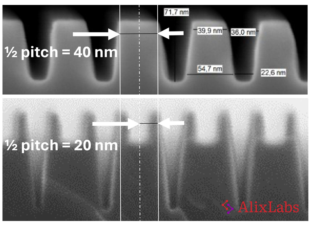
Picture: Scanning electron microscopy (SEM) images of amorphous silicon lines before (top) and after the APSTM process: nominal 40nm line width and 40nm half-pitch converted to lines with width below 15nm and a half-pitch of 20nm.
AlixLabs’ offering includes its APS technology that already allows for etching of feature sizes comparable to those of today’s 3nm-class chips with the company’s own equipment. With other proprietary ALE processes, AlixLabs can also contribute to RF and power IC gallium nitride (GaN) and silicon carbide (SiC) workflows, with pattern transfer, precision etching and surface roughness reduction for wafers.
“The semiconductor industry is facing a big challenge with regards to sustainability and rising costs to manufacture leading-edge semiconductors. We propose etching instead of costly EUV [extreme ultraviolet] lithography, and our demonstrations show that we can help produce sub-3nm chips at 35–50% lower costs per wafer pass than by using EUV,” says CEO Jonas Sundqvist. “While we target the leading-edge logic and memory producers with APS, our technology also makes it possible for foundries who have given up pursuing sub-20nm production to scale down in a cost-effective way.”
The Vinnova grant will be used by AlixLabs to accelerate the commercialization of its APS technology by deepening customer engagement and conducting demonstration projects. These demos will be carried out both at AlixLabs’ facilities and on customer platforms, showcasing the practical advantages of APS. This approach is expected to advance the Technology Readiness Level (TRL) of the firm’s solutions, paving the way for broader industry adoption and reinforcing AlixLabs’ commitment to delivering cost-effective scaling solutions for semiconductor manufacturing.
AlixLabs gains SEK2.5m grant from Sweden’s Vinnova
EU Intellectual Property Office grants trademark registration for AlixLabs’ APS process


