News: Microelectronics
22 November 2024
MESFETs on single crystal aluminium nitride substrate
Arizona State University (ASU) in the USA reports on high-voltage aluminium nitride (AlN) metal–semiconductor field-effect transistors (MESFETs) on single-crystal AlN substrates [Bingcheng Da et al, Appl. Phys. Express, v17, p104002, 2024]. The researchers claim their work as the first report of “AlN transistors via homoepitaxial growth on native substrates”.
The team comments: “The devices showed good saturation and pinch-off behavior with high maximum Ids, gm and on/off ratio compared with AlN-on-sapphire devices without complicated contact layers.”
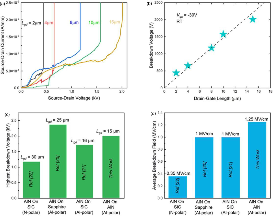
AlN has the highest breakdown electric field, 12MV/cm, compared with potential ultrawide-bandgap (UWG) competitors, such as gallium oxide and diamond, putting it in the frame for future high-voltage, high-power applications. The best average breakdown electric field of the ASU devices was an order of magnitude down on the maximum possible, at 1.25MV/cm. However, this was still a 25% improvement on other reported AlN transistors produced on hetero-structures on foreign substrates such as sapphire or silicon carbide (SiC).
The use of homo-epitaxial AlN-on-AlN substrate enables lower defect densities to be realized. This is one hurdle jumped in the race to achieve high-performance power devices. Other challenges include improving the doping effectiveness for low-resistance channels, and enhancing the conductivity through the (desired) ohmic source/drain electrode contact.

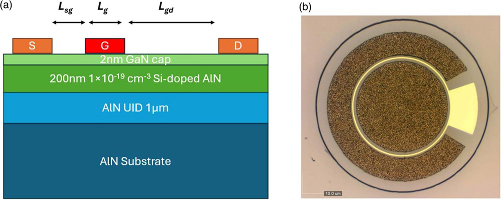
Figure 1: (a) Schematic cross-section and (b) top-view microscope image of fabricated AlN MESFET.
The researchers used AlN substrates with a 103/cm2 dislocation density for the AlN MESFETs (Figure 1). The epitaxial structure was grown using metal-organic chemical vapor deposition (MOCVD) from trimethyl-aluminium (TMAl), ammonia (NH3), and silane (SiH4) precursors. The growth conditions were 1250°C temperature and 20Torr pressure. A gallium nitride cap layer was included in the growth to protect the AlN from atmospheric oxidation. The resulting material demonstrated a 0.4nm surface roughness, and dislocation density of order 104/cm2.
The team comments: “Compared with heteroepitaxial AlN on sapphire, homoepitaxial AlN on single-crystal AlN substrates had three orders of magnitude lower dislocation density, which can improve AlN device performance.”
The MESFET devices were fabricated using inductively coupled plasma reactive ion etch to a depth of 700nm into the AlN resistive buffer layer; deposition of annealed titanium/aluminium/nickel/gold ohmic contact source/drain (S/D) electrodes; and deposition of the nickel/gold gate.
The source–gate (sg) and gate lengths were both 2μm. The gate–drain (gd) length was varied (2–15μm) to study the trade-off between on-resistance and breakdown voltage. A longer Lgd increases on-resistance (bad), but lowers the peak electric field, increasing the breakdown voltage (good).
Electrical characterization between room temperature (RT=298K) and 473K showed reduced contact resistivity (ρc) and sheet resistance (Rsh) at higher temperatures: 0.77Ω-cm2 and 2.4x10⁷Ω/square at RT; and 0.15Ω-cm2 and 6.6x10⁵Ω/square at 473K, respectively.
The researchers comment: “The reduction in contact resistivity at high temperatures is likely due to easier passage of the thermally excited electrons through the metal/AlN interface by tunneling through an effective thinner potential barrier and/or thermionic emission.”
The 2μm Lgd MESFETs demonstrated a normally-on operation with a pinch-off at gate (Vgs) voltages less than −20V. For many applications a positive threshold, giving normally-off performance, is preferred, but AlN transistor development is presumably at too early a stage to think about that!
The maximum drain current (Ids) at RT reached 56μA/mm at 9V Vgs — “6 times higher than that of the reported AlN-on-sapphire MESFETs,” according to the team. The researchers go on to explain: “The increase in Ids could be attributed to the lower sheet resistance of the homoepitaxial AlN layer (2.4x10⁷Ω/square) compared with that of AlN layers on sapphire (8x10⁷Ω/square).” The maximum transconductance reached 1.49μS/mm.
The devices with 8μm Lgd showed the lowest RT off current of 3.3x10⁻⁸A/mm, giving an on/off ratio of 700. While low compared to commercial transistors in other material systems, this value is around 6x higher than for previous AlN-on-sapphire MESFETs, the team says.
In experiments over the full 298–473K temperature range, the reverse gate leakage through the Schottky gate was less than 1.7x10⁻⁹A/mm at −20V Vgd. The researchers report: “Reverse gate leakage current was almost constant, showing stable gate control with increasing temperature.”
The maximum drain current and transconductance increased between RT and 473K: from 2.06x10⁻⁵ to 3.42x10⁻⁴A/mm; and from 1.19x10⁻⁶ to 2.45x10⁻⁵mS/mm, respectively.
The researchers explain: “There was a significant increase in the electron concentration from 1x10¹⁵ to 5.6x10¹⁷/cm3 as the temperature increased from RT to 500°C with a relatively small reduction in mobility from 156 to 52 cm2/V-s. Consequently, the electrical conductance of the n-type AlN layer increased with rising temperature, leading to enhanced output performance at high temperatures. This is in contrast with conventional wide-bandgap semiconductors like GaN and SiC, where their overall forward performance of FETs based on these semiconductors deteriorates with increasing temperature due to a dominant reduction in electron mobility by phonon scattering.”

Figure 2: (a) Off-state breakdown characteristics with different Lgd. (b) Breakdown voltages versus Lgd. Comparison of reported AlN MESFETs in terms of (c) breakdown voltages and (d) average breakdown fields.
Off-state breakdown at RT (Figure 2) occurred through destructive failure at the device edges. The researchers state that the breakdown came from electric field crowding effects. The gate potential was −30V. The longest 15μm Lgd device broke at 2010V, the second highest on a comparison chart, behind a 25μm Lgd transistor on sapphire, breaking at 2.3kV. However, the ASU structure enabled a 25% higher average electric field (1.25MV/cm) to be reached. The shorter Lgd of the ASU device allows a higher conductivity for target 2kV breakdown rating.
Looking ahead, the ASU teams reports: “Further work on implementing electric field management approaches such as field plates is underway to improve the breakdown field.”
The author Mike Cooke is a freelance technology journalist who has worked in the semiconductor and advanced technology sectors since 1997.


