News: Microelectronics
7 November 2024
Double-heterostructure gallium nitride for 5G FR2 mobile handsets
Researchers based in Singapore claim a record saturated output power (Psat) for gallium nitride (GaN) on silicon (Si) high-electron-mobility transistors (HEMTs) aimed at low-voltage (LV) high-frequency performance [Hanchao Li et al, IEEE Electron Device Letters, published online 21 October 2024].
The team, from the Nanyang Technological University, the National GaN Technology Centre (NGTC), the Institute of Microelectronics (IME), the Singapore-MIT Alliance for Research and Technology, and the National University of Singapore, comment on their double-heterostructure (DH) as opposed to conventional single-heterostructure (SH) device: “Till date, all the reported demonstrations are achieved using SH epitaxies, and the majority use deeply scaled gates (Lg<100nm). In comparison, the proposed transistor achieves excellent performance using a longer Lg of 120nm, and conventional ohmic and gate processes.”
The researcher see great potential particularly for high transmit power in fifth-generation (5G) frequency range 2 (FR2) mobile handsets targeting high uplink/downlink rates (peak of 10/20gigabits/s). FR2 covers 24.25–71.0GHz, while FR1 is less than 7GHz. The gap 7–24.25GHz has been proposed, but not approved, as a 5G FR3. The GaN/Si HEMT option offers “the merits of GaN in power amplification with availability of wafers up to 300mm,” according to the team.
The search for high-power, high-frequency performance tends to need shorter gate lengths, but such devices are negatively impacted by a range of “short-channel effects” (SCEs) that downgrade expectations of improved frequency performance from transistor scaling models.
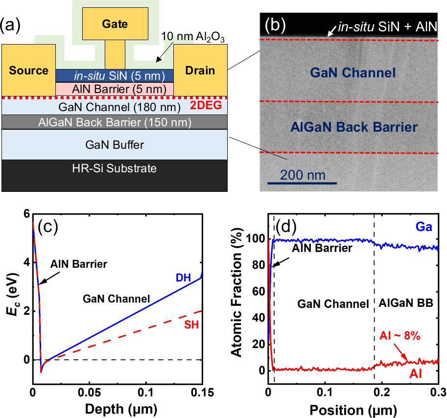
The DH structure consisted of a GaN channel surrounded by aluminium nitride (AlN) top and AlGaN bottom barriers. SH devices just have the top barrier confining carriers to the channel.
The researchers comment on the DH HEMT structure: “Previous work has studied this heterostructure for higher-voltage power amplification. However, to the best of the authors’ knowledge, the potential of DH HEMTs in LV power amplification remains unexplored.”

Figure 1: (a) Schematic cross-section of AlN/GaN/AlGaN DH HEMT. (b) Scanning transmission electron microscope (STEM) image of heterostructure. (c) Band diagrams of DH versus conventional SH heterostructures. (d) Elemental composition of heterostructure from energy-dispersive x-ray spectroscopy (EDX).
The double-heterostructure HEMT material was grown on high-resistivity silicon (HR-Si), using metal-organic chemical vapor deposition (Figure 1). The structure included an in-situ silicon nitride (SiN) layer to reduce gate leakage through the thin AlN barrier layer. The buffer was 1μm thick.
The AlGaN back barrier had an Al content of 8%. The back barrier was designed to increase carrier confinement in the channel region of the device, as suggested by 1D Schrodinger−Poisson band-structure calculations. The sheet carrier density was 1.7x10¹³/cm2 and the mobility was 1400cm2/V-s, according to Hall measurements. The sheet resistance was 260Ω/square.
Device fabrication started with the source/drain contacts consisting of titanium/aluminium/nickel/gold, followed by plasma mesa etching for isolation. The T-gates consisted of nickel/gold. The HEMT was completed by a thin 10nm atomic layer deposition layer of aluminium oxide (Al2O3) as passivation.
The researchers comment: “The thin ALD-Al2O3 passivation layers could reduce the parasitic capacitance, while avoiding plasma-induced damage associated with PECVD processes, thereby offering more effective protection to the device’s access region.”
The dimensions of the tested device included 120nm gate-length, 690nm spacings between the centrally placed gate from the source and drain contacts, and 2x16μm gate width. The relatively small width was designed to avoid self-heating effects, allowing better assessment of the intrinsic performance of the DH transistor design.
The maximum drain current was 1.9A/mm with an ON-resistance of 1.5Ω-mm, and peak transconductance of 0.66S/mm. The threshold was negative (−2.9V), indicating normally-on/depletion-mode operation. The three-terminal breakdown voltage was 49V, giving an estimated breakdown electric field of 0.327MV/cm.
The researchers comment: “The breakdown mechanism is attributed to source−drain punch-through, which benefits from the design of the floating gate structure and the high quality of in-situ SiN.”
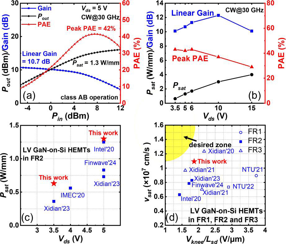
The small-signal frequency performance measurements resulted in 145GHz cut-off (fT) and 195GHz maximum oscillation (fmax) frequencies at 5V bias (Vd) and -2.5V gate potential (Vg). The fT/fmax values were in the respective ranges 140–150/190–200GHz for biasing above 3V. The frequency–gate-length products were considered high at 17.4GHz-μm and 23.4GHz-μm for the cut-off and maximum oscillation, respectively. Multiplying the cut-off product by 2π gave a rough estimate for the carrier saturation velocity of 1.1x107cm/s.

Figure 2: (a) Power sweep. (b) Load-pull performance versus Vds. (c) Benchmark of Psat versus Vds for LV 5G FR2 operation. (d) Comparison of vsat versus Vknee (normalized by source/drain separation) for reported low-voltage GaN-on-Si transistors in FR1, FR2 and FR3.
The large-signal power capability (Figure 2) was assessed using on-wafer load-pull measurements at 30GHz fundamental frequency continuous wave (CW). The saturated output power (Psat) was 1.3W/mm with 32% power-added efficiency (PAE) and 3.7dB gain. The peak PAE was 42% with an output power (Pout) of 1.1W/mm and 7.3dB gain.
Reducing the bias to 3.5V enabled a slightly higher peak PAE of 43% with 0.52W/mm Pout and 7.2dB gain.
The Psat value increased at an approximate linear rate up to 15V bias, reaching 4.0W/mm. The researchers comment: “The peak PAE decreased, mostly due to increased effect of traps and limited available load impedance tuning results of non-optimal matching condition.”
The researchers see room for improvement in optimizing the passivation, more aggressive scaling, and ohmic contact design. They also suggest that achieving a positive threshold voltage, and hence normally-off/enhancement-mode operation, would be beneficial for handset deployment.
The author Mike Cooke is a freelance technology journalist who has worked in the semiconductor and advanced technology sectors since 1997.


