News: Microelectronics
14 November 2024
Boron enables AlN on silicon growth without cracks
Researchers based in Saudi Arabia and Taiwan report on the ability of boron (B) added to aluminium nitride (AlN) to allow the growth of thicker AlN layers on silicon (Si) without cracking [Mingtao Nong et al, Appl. Phys. Lett., v125, p172107, 2024].
The BAlN was used as a buffer layer. The thickness of AlN achieved without cracking was 520nm, the thickest reported, according to a benchmark graph (Figure 1) presented in the paper.

Figure 1: Benchmarks across a range of studies of MOCVD AlN films on Si (111) substrates: thickness versus full-width at half maximum (FWHM) values for x-ray rocking curves (XRC) from (a) (002) and (b) (102) planes.
The researchers from King Abdullah University of Science and Technology (KAUST) in Saudi Arabia and National Yunlin University of Science and Technology in Taiwan comment: “Employing TEB [triethyl-boron] flow during buffer layer deposition not only enables achieving a maximum thickness of 520nm without cracking but also results in the lowest full-width at half maximum (FWHM) values for both 002 and 102 planes compared to those in other studies.”
The team sees potential for high-electron-mobility transistors (HEMT), high-power devices, piezoelectric sensors, and solar-blind photodetectors. The ultrawide bandgap of AlN (6eV) increases the critical electric field before breakdown, potentially allowing smaller devices to handle larger voltages thus achieving higher-power-density capability.
Although AlN would preferably be grown on native AlN substrates, such material is much more expensive than silicon. Further, an attractive possibility for AlN/Si would be highly integrated AlN devices coupled to mainstream silicon integrated circuitry.
The need for buffer layers between Si and AlN arises from lattice and thermal expansion mismatches of 19% and 43%, respectively. AlN growth is carried out at very high temperature in the range 900–1200°C. When cooled, such material tends to crack as the Si and AlN lattices contract at different rates.
The researchers comment: “The introduction of such a BAlN buffer layer presents two primary advantages: it significantly delays coalescence, thus reducing accumulated stress; and it compensates for the tensile stress caused by the larger lattice parameter of silicon compared to AlN by introducing compressive stress from the smaller lattice parameter of BAlN.”
The AlN layers were grown on 2-inch silicon by metal-organic chemical vapor deposition (MOCVD). The precursors were trimethyl-aluminium (TMAl) and ammonia (NH3). Boron modification was achieved by adding triethyl-boron (TEB) to the inputs.
Three samples were grown. The buffer was grown at 950°C with a V/III ratio of 16,500 for 10 minutes. The samples 1–3 were distinguished by the B/III mole flow ratio: 0%, 20% and 40%, respectively. Sample 1 was thus an AlN reference without B modification.
On top of the buffer the main AlN layer was grown at a high temperature of 1150°C at a 110 V/III ratio. The reactor pressure was maintained at 7.5kPa throughout buffer and AlN growth.
Reflectance measurements made ‘in-situ’ during the growth showed different coalescence behaviors of the initial islands of III-nitride material: around 200nm and 400nm for samples 1 and 2, respectively. The researchers comment: “This delayed coalescence suggests a reduction in residual stress and defects.”
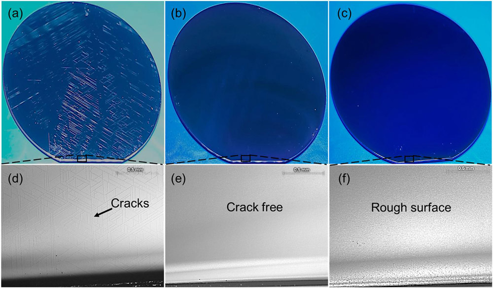
Sample 3 suffered from insufficient coalescence and resulted in a rough surface morphology.
Another indicator of strain was the radius of curvature of the samples. By the end of the growth the curvatures reached 69km, 44km and 29km for samples 1–3, respectively. “The incorporation of BAlN can effectively minimize wafer warpage and alleviate tensile stress in AlN films,” the team writes.
The final sample 1 with AlN buffer showed cracking effects (Figure 2). The BAlN buffer samples avoided cracking, but sample 3 had a rough surface.

Figure 2: Photographs and optical microscopy images (500x) for samples 1 (a, d), 2 (b, e), and 3 (c, f).
The final surface roughness of sample 3 was 22.89nm, according to atomic force microscopy (AFM). The corresponding figures for the samples 1 and 2 were 0.45nm and 0.54nm.
Sample 2 combined the desirable features of no cracking and a smooth surface. The composition of the BAlN buffer in sample showed a B content around 4%, according to secondary-ion mass spectroscopy (SIMS). The buffer thickness was about 30nm, and the total thickness of the AlN/BAlN structure was around 520nm. Growth-rate monitoring during the MOCVD suggested that all the samples would have a similar total thickness.
The researchers comment: “Obviously, the actual B% in the buffer layer of sample 2 is significantly lower than the expected B/(B+Al) ratio of 20% introduced into the reactor. This discrepancy is attributed to the difficulty in incorporating B into the AlN layer.”
AFM measurements on the buffer layers, showing an increase roughness of BAlN material, suggested that boron increases the nucleation site size from which crystal BAlN grows, first separately, and then coalesced into the desired AlN layer. Before coalescence, the islands increase roughness due to uneven growth rates and irregular merging.
The early coalescence in the sample 1 with only AlN as buffer accumulates stress into a too narrow region, creating the conditions for cracking.
Table 1: Material characterizations: densities (D) of screw and edge dislocations, and biaxial stress (σ).
Sample |
Dscrew |
Dedge |
σ |
| 1 | 1.76x10⁹/cm2 | 17.3x10⁹/cm2 | −2.67GPa |
| 2 | 1.04x10⁹/cm2 | 10.2x10⁹/cm2 | −1.63GPa |
| 3 | 6.50x10⁹/cm2 | 18.7x10⁹/cm2 | −1.30GPa |
The researchers used x-ray analysis to derive the dislocation densities, and Raman spectroscopy for biaxial stress (Table 1). The sample 2 with BAlN buffer showed reduced dislocation density and moderate tensile stress to avoid cracking, compared with the other samples.
The author Mike Cooke is a freelance technology journalist who has worked in the semiconductor and advanced technology sectors since 1997.


