News: Microelectronics
14 November 2024
Toshiba ships early test samples of bare die 1200V SiC MOSFET
Toshiba Electronic Devices & Storage Corp has developed new 1200V silicon carbide (SiC) MOSFETs with an innovative structure that delivers both low on-resistance (RDS(ON)) and high reliability. The devices are particularly suited to automotive applications such as traction inverters. They are now available and shipping as early test samples in bare die format, allowing users to customize the bare die to meet their specific design needs and realize solutions for their applications.

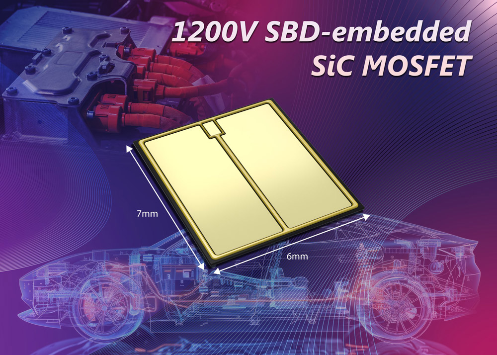
Picture: Toshiba’s X5M007E120, a bare die 1200V SiC MOSFET that delivers both low on-resistance and high reliability for automotive traction inverters.
The reliability of typical SiC MOSFETs is degraded by increased on-resistance when its body diodes are bipolar energized during reverse conduction operation. Toshiba’s new SiC MOSFETs alleviate this issue by using a device structure that embeds Schottky barrier diodes (SBDs) into the MOSFET to inactivate body diodes. However, positioning the SBDs on the chip reduces the area available for channels that determine the resistance of MOSFET on-operation, increasing the chip’s on-resistance.
The SBDs embedded in the X5M007E120 are arrayed in a check pattern (rather than the typically used striped pattern), which effectively suppresses bipolar energization of the device’s body diodes, while improving the upper limit of unipolar operation to about twice the existing area, even when taking up the same SBD mounting area (compared with Toshiba’s product using a striped pattern). Compared with the striped array, channel density is also improved, and on-resistance per unit area is reduced by 20–30%. This improved performance (low on-resistance while maintaining reliability against reverse conduction operation) can save energy in inverters used for motor control, such as automotive traction inverters.
Reducing RDS(ON) in a SiC MOSFET can cause excess current flow through the MOSFET during short-circuit, reducing short-circuit durability. Enhancing the conduction of the embedded SBDs to improve the reliability of reverse conduction operation also increases current leakage during short-circuit, again decreasing short-circuit durability. The new bare die has a deep barrier structure that suppresses excessive current in the MOSFET section and leakage current in the SBD section during short-circuit operation. This improves its durability during short-circuit conditions while maintaining high levels of reliability against reverse conduction operation.
The new X5M007E120 has a drain–source voltage rating (VDSS) of 1200V and is rated for a drain current (ID) of 229A continuously, with 458A for pulsed operation (ID Pulse). The on-resistance (RDS(ON)) is as low as 7.2mΩ (typical, at VGS=+18V, Ta=25°C) and 12.1mΩ (typical, at VGS=+18V, Ta=175°C). Also, the device can operate with channel temperatures (Tch) as high as 175°C. The devices are AEC-Q100 qualified for automotive applications.
Toshiba expects to ship engineering samples of the new X5M007E120 during 2025, and to start mass production in 2026. In the meantime, it will explore further improvement to device characteristics.
Toshiba’s launches 1200V third-generation SiC Schottky barrier diodes
Toshiba releases third-generation SiC MOSFETs with reduced switching losses


