News: Suppliers
22 October 2024
Comptek completes installation of Kontrox-powered 200mm wafer pilot line
Comptek Solutions Oy of Turku, Finland (which specializes in III-V compound semiconductor quantum surface engineering) has completed the installation of its pilot line, after a two-year project funded by the European Innovation Council (EIC).
The pilot line integrates Comptek’s proprietary Kontrox passivation technology with other widely used industry techniques such as atomic layer deposition (ALD), delivering a proven, scalable solution for industrial manufacturing specifically targeting power electronics and optoelectronic applications.
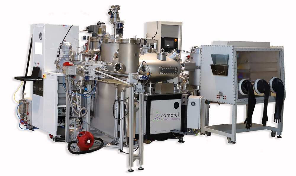
Designed to validate Comptek’s Kontrox passivation technology on up to 200mm substrates, this cluster tool integrates the Kontrox passivation process with industry-standard methods, featuring a plasma-enhanced ALD (PE ALD) module, along with advanced functionalities for wet etching and chemical processing in a controlled inert gas atmosphere. With continuous processing that maintains vacuum between different process steps, the system offers flexibility in developing complex passivation solutions that meet the most demanding requirements, it is claimed, ensuring superior chip performance and long-term reliability for high-performance semiconductor applications.

Picture: Comptek’s pilot line.
“The pilot line we’ve developed through the EIC-funded ‘Enlight’ project is a testament to our commitment to pushing the boundaries of passivation technology,” says CEO & co-founder Vicente Calvo Alonso. “The possibility to combine our unique Kontrox passivation technique with advanced ALD capabilities allows us to deliver highly customizable and optimized solutions, designed to overcome the challenges and fulfill the needs of power electronics and optoelectronic manufacturers,” he adds. “With this pilot line, we are excited to offer our customers the opportunity to tailor the processes to their exact production requirements, helping them achieve unprecedented performance for their device applications.”
The pilot line integrates Comptek’s Kontrox process with ALD technology, implemented using Veeco’s PE-ALD FIJI 200 system. This combination provides what is said to be a transformative approach to minimizing surface defects and creating a sharp III-V dielectric interface. The result is said to be superior interface quality, crucial for maximizing chip performance and optimizing yields in a wide range of semiconductor applications, from sidewall passivation layers for micro-LEDs to complex gate stack dielectrics for power transistors.
Through the EIC Accelerator funding, the Comptek was able to refine its core processes and validate its passivation technology for large-scale industrial manufacturing. “The EIC’s funding and guidance have enabled us to build a turnkey passivation solution for larger substrates, allowing Comptek Solutions to advance the applicability of our technology to the industrial scale,” comments Vicente. “This achievement would not have been possible without the EIC’s belief in the potential of our innovations and their commitment to driving technological breakthroughs in Europe.”
The compound semiconductor substrate market is reckoned to be growing at 17% annually from 2023 to US$3.3bn in 2029, driven by increasing demand from sectors such as automotive, communications and consumer electronics, with growth in power electronics fuelling the transition to larger substrates like 200mm wafers for silicon carbide (SiC) and gallium nitride on silicon (GaN-on-Si). Meanwhile, the rising use of 150mm indium phosphide (InP) in datacoms and 200mm gallium arsenide (GaAs) and sapphire in micro-LED displays is driving further demand for advanced semiconductor technologies, Comptek notes. These trends underscore the need for high-quality passivation to ensure optimal performance and reliability in power and optoelectronic applications while promoting sustainable semiconductor manufacturing, the firm adds.
Comptek says that its EIC-funded pilot line, with its potential for next-level compound semiconductor-based substrate passivation, has already attracted significant interest. Several major manufacturers have already scheduled trial runs to explore its top-tier capabilities for their specialized production needs, and the company’s capacity for 2025 is already fully booked.
Comptek secures €8m in Series A funding round
Riber and Comptek partner to commercialize Kontrox technology
Comptek raises €450,000 for Kontrox technology to passivate oxidized III-V surfaces


