News: LEDs
11 October 2024
Double V-pits enhance red InGaN LED internal quantum efficiency
Dongguan University of Technology and Dongguan Institute of Opto-Electronics Peking University in China have reported on improving the internal quantum efficiency (IQE) of indium gallium nitride (InGaN) red light-emitting diodes (LEDs) by using a double V-pit structure [Chuanyu Jia et al, Optics Express, v32, p36489, 2024].
The IQE reached 21.5%, compared with 10.5% for a single V-pit structure at wavelengths of 613nm and 612nm, respectively. [These wavelengths are more precisely orange, 590–625nm, rather than red, 625–750nm.] The improvement in external quantum efficiency (EQE) was less impressive: 6.2%, compared with 5.3%. Recent reports typically have EQEs at about 6%, although Nanchang University has reported a 24% wall-plug efficiency for a 608nm InGaN red LED grown on silicon.
The exploitation of red-emitting III–nitride materials to provide red–green–blue displays is hampered by red InGaN’s low IQE relative to blue- and green-emitting alloys at 90% and 60%, respectively.
The researchers believe that their double V-pits layer structure relieves the compressive strain of InGaN multiple quantum wells (MQWs), reducing the influence of the piezoelectric polarization field and thus improving the IQE.
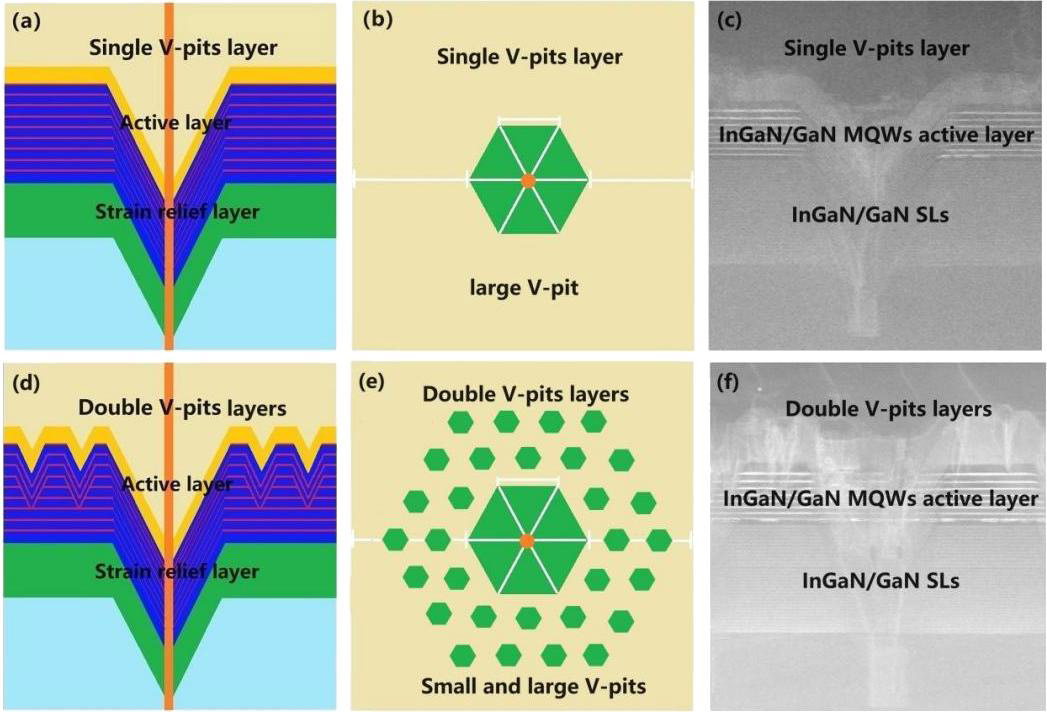
The LEDs were grown on patterned sapphire substrate (PSS), using metal-organic chemical vapor deposition (MOCVD). Samples with single and double V-pit structures were grown in the active MQW region (Figure 1).

Figure 1: Cross-sectional LED views: (a) sample A with single, and (d) sample B with double, V-pit layers; plan views: (b) sample A, and (e) sample B; transmission electron microscope (TEM) images: (c) sample A, and (f) sample B.
The large, sparse V-pits were created by a low-temperature (LT) growth of an interlayer between the strain relief and MQW structures. The strain relief consisted of 100nm GaN and a 32-period 5nm/2nm InGaN/GaN superlattice grown at low temperature (820°C). The strain relief reduced the density of threading dislocations. It was at these dislocations that the large V-pits formed.
The dislocation/large V-pit density was about 108/cm2. One factor that enabled this low dislocation density was the use of a 25nm sputtered aluminium nitride (AlN) layer for nucleation on the PSS before the MOCVD processing.
The MQW structure consisted of 5-periods of In0.2Ga0.8N/GaN ‘green’-emitting layers, and 3-periods of In0.4Ga0.6N/GaN ‘red’. The GaN was grown at 830°C and 810°C for the green and red structures, respectively. The corresponding InGaN growth temperatures were 720°C and 700°C. These temperatures are compromises needed to achieve the required crystal quality (high temperature preferred) and indium incorporation (low temperature preferred).
The second small V-pit layer for sample B was achieved by altering the growth conditions of the 5-period green MQW. In particular, the GaN barrier layers were grown at 750°C. The InGaN was grown at 720°C, as for the single V-pit sample A structure.
The lower temperatures resulted in slower growth. The researchers report that the total thickness of the low-temperature layers was reduced from 324nm in sample A to 62nm in sample B.
The materials were fabricated into 100μmx200μm LEDs.
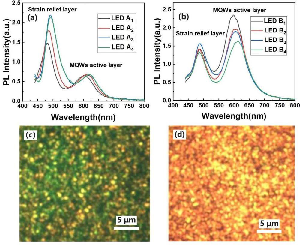
The room-temperature PL red emission was a factor of 245% greater in sample B, compared with sample A (Figure 2). Sample A showed a mix of red and green regions under a microscope, with the green tending to dominate. The researchers attribute this to “serious InGaN phase segregation in sample A2, in which the low-indium-component phase emits green light, and the high-indium-component phase emits red light.”

Figure 2: Room-temperature photoluminescence spectra of LED samples: (a) A1–4 and (b) B1–4. Fluorescence images of (c) A2 and (d) B4 taken under identical 405nm laser excitation.
There is also some color conversion of green to red light in the red MQW layers.
The team comments: “Compressive strain in the red MQWs of LED sample B can be more effectively released as compared to that of LED sample A by opening small V-shaped pits with high density in the red MQWs region. The small V-pits divides the large continuous area of QW into small isolated pieces, which prevents the transmission of strain, converts the long-range strain on the QW into separated local strain, and makes the strain on the QW smaller. The side-wall surface of the V-shaped pit, as a free interface, also plays a role in the release of strain.”
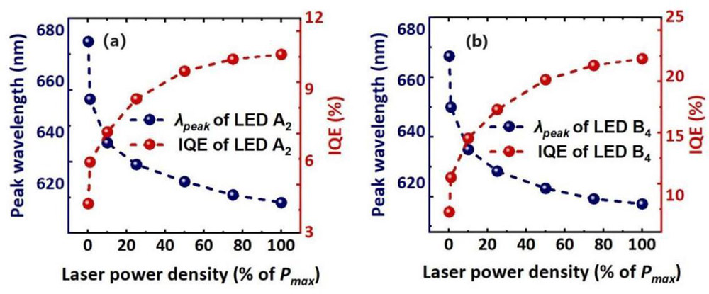
The IQE was estimated by comparing the photoluminescence (PL) responses at room temperature (300K) and 5K (assumed to have 100% IQE). The researchers used a 532nm laser excitation to focus on the red rather than green peak wavelength and IQE of the samples (Figure 3).

Figure 3: Peak wavelength and IQE of samples (a) A2 and (b) B4.
The maximum laser excitation power density was 105/cm2. The peak IQEs of samples A2 and B4 were 10.5% at 613nm and 21.5% at 612.1nm, respectively.
The improvement in peak EQE of electroluminescence was less impressive, increasing from 5.3% (sample A) to 6.2% (sample B) at 1A/cm2. The researchers explain: “The introduction of high-density small V-shaped layer in the active layer will affect the growth of following p-type layer and generate new leakage channels in the active region, which has a negative impact on electroluminescence (EL) of LED sample B.”
Both devices show drooping intensity beyond the low 1A/cm2 current density. The researchers hope that optimizing the p-type layer growth will control leakage and improve EL intensity in future work.
https://doi.org/10.1364/OE.533052
The author Mike Cooke is a freelance technology journalist who has worked in the semiconductor and advanced technology sectors since 1997.


