


News: Microelectronics
23 September 2024
Tunnel-junction-enabled GaN heterojunction bipolar transistors
Ohio State University (OSU) in the USA reports on using tunnel junctions (TJs) rather than p-type base contacts for improving the performance of III–nitride heterojunction bipolar transistors (HBTs) [Chandan Joishi et al, IEEE Transactions On Electron Devices, published online 5 September 2024]
The use of p+/n+ TJs (Figure 1) enables all the terminal contacts — emitter, collector, and base — of the HBT to be with metals suitable for n-type gallium nitride (GaN). In general, p-type GaN has a much higher resistivity than n-type.
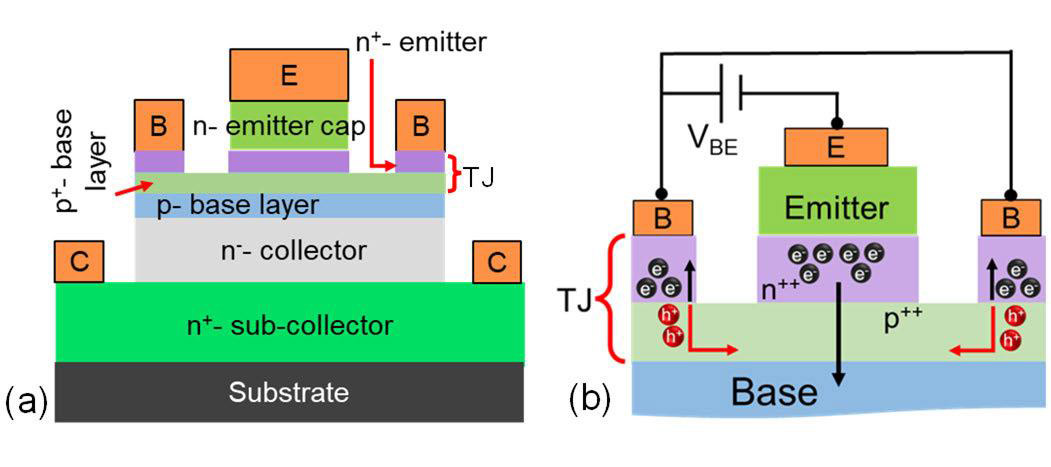
Figure 1: (a) Two-dimensional schematic of proposed III–nitride TJ HBT with n- and p-type epilayers. (b) Zoom-in schematic of emitter–base region displaying carrier flow (electrons, black; holes, red) in active mode (VBE > 0).
The researchers comment: “This novel approach to HBT design significantly advances the current field of III–nitride HBTs for the next-generation radio frequency (RF) and mm-wave applications by circumventing the need to fabricate p-type contacts on the base as well as eliminating regrowth of the emitter/base epilayers.”
The team explains the potential benefit of the TJ structure: “During the forward active mode of operation of the HBT, the forward-biased emitter–base junction injects minority electrons into the base, while the reverse bias at the n+/p+ base contact acts like an ohmic contact and injects holes into the base. Thus, the same n+–p+ layer behaves as both the emitter/base junction and the base TJ contact layer.”
HBT development has tended to lag that of field-effect devices such as high-electron-mobility transistors (HEMTs) “due to several reasons, most of which are related to the resistance associated with the p-type base contact layer,” the team reports, adding: “Despite the great success of GaN HEMTs, there are still some factors that make it worthwhile to pursue research that could overcome the challenges associated with GaN HBTs.”
Among the factors potentially favoring HBT is the positioning of peak electric fields away from surfaces, where efficiency-sapping recombination rates tend to increase due to surface damage from etch processing. HEMTs also suffer from concentration of the current flow within small volumes, relatively to HBTs. For HBTs, this could result in better thermal management and realization of higher carrier velocities, improving high-frequency performance.
These benefits, and others, have yet to be realized in actual devices that fall far short of predictions. One example the OSU team points to is a reported 500GHz-V Johnson’s figure of merit estimate, measuring carrier velocities and breakdown performance, being an order of magnitude lower than the ~5THz-V theory prediction from material properties.
The material used for the HBTs was grown at a rate of ~4nm/min by plasma-assisted molecular beam epitaxy/PA-MBE (Figure 2). The AlGaN regions in the emitter stack were linearly graded up to 20% and back down to 0%. The researchers report: “We used a graded AlGaN/GaN emitter region to improve the emitter injection efficiency.”
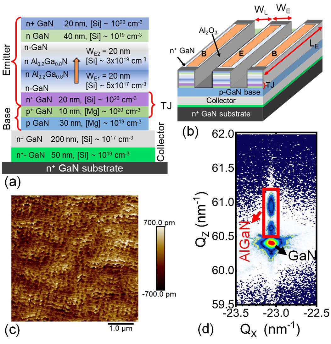
Figure 2: (a) Two-dimensional schematic of as-grown GaN TJ HBT. (b) Three-dimensional schematic of fabricated device. (c) Atomic force microscope (AFM) image of as-grown surface over 5μmx5μm field. (d) X-ray diffraction (XRD) reciprocal space map (RSM) of as-grown epitaxial stack.
The as-grown material demonstrated a root-mean-square roughness of 0.2nm in AFM analysis. The RMS measurements showed the desired fully strained growth.
Fabrication began with plasma-enhanced chemical vapor deposition (PECVD) of a 250nm sacrificial silicon dioxide (SiO2) layer. Photolithography and dry/wet etch opened windows in the SiO2 hard mask for further plasma etch of the III–nitride epitaxial layers, defining the collector region.
The SiO2 mask was then patterned again for III-nitride material reactive-ion etch (RIE)/inductively coupled plasma (ICP) etch to give interdigitated stripes, isolating the base and emitter regions. The team comments: “The emitter–base isolation was achieved through a BCl3/Cl2-based low-power (~5W RIE, 40W ICP) etch recipe to minimize etch damage.”
The stripes were etched down to the p+ GaN to avoid potential problems from etch variation, which could potentially reach ~4nm.
The emitter–base contacts were aluminium/nickel/gold. Metal deposition was followed by atomic layer deposition (ALD) of aluminium oxide (Al2O3) as both sidewall passivation and isolation layer between the emitter–base bond pads, formed by Ni sputtering into windows etched into the Al2O3.
Measurements on a 3μmx1.4μm emitter (LExWE) device with 9 emitter stripes showed a 4.5V base–collector current (IB/IC) crossover at 0V VCB(Figure 3). The maximum current gain was less than 4 at current densities greater than 10kA/cm2.
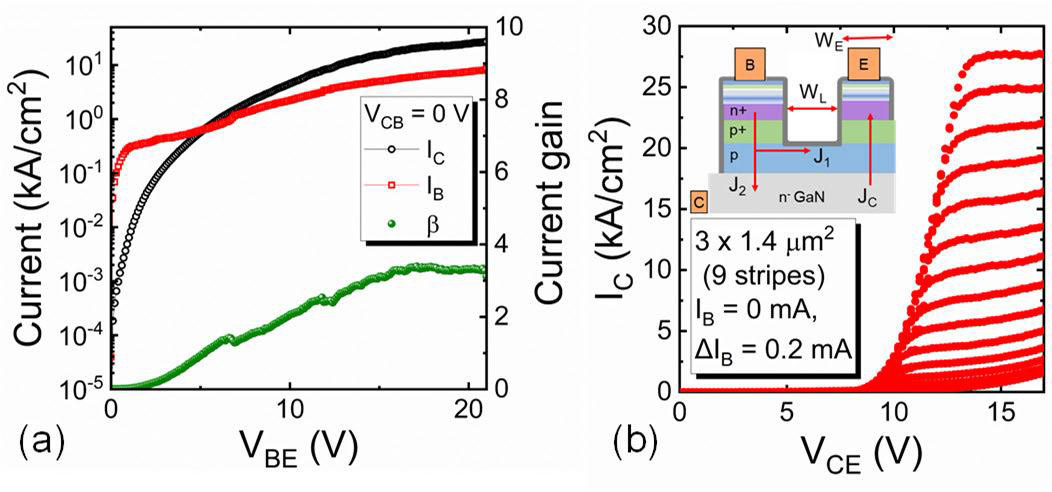
Figure 3: (a) Gummel plot with 0V VCB and (b) common emitter output current–voltage characteristics (IC–VCE), and inset schematic of current flow path.
The crossover was higher than the figure predicted in the design simulations (3V). The researchers blame recombination due to the non-radiative Shockley–Read–Hall (SRH) mechanism, based on the non-observation of light emission during operation. This recombination results in a “shorter minority carrier lifetime in the base and diminishes the base transport factor of the device,” the team suggests. The researchers estimate base voltage drop to result from a resistance of order 400kΩ/square.
The collector current reached as high as 28kA/cm2 density at more than 12V VCE.
The researchers comment: “To improve VCE,offset, improvement in current gain, base conductance, and scaling of WL [stripe separation] is essential. Nevertheless, the output characteristics show a sharp rise in output current density after VCE,offset, implying low ON-resistance during device operation.”
The team suggests four potential enhancements:
1) polarization engineered thin base layers to improve base conductivity;
2) optimized TJ growth conditions using MBE and/or metal-organic chemical vapor deposition (MOCVD) to improve device leakage and mitigate non-ideal recombination by enhancing material quality, increasing minority carrier lifetime and improving the base transport factor;
3) employing alternate approaches, such as ion implantation, to isolate the devices and adjacent emitter–base terminals, mitigating impact of plasma etch damage to emitter–base access region; and
4) sub-micrometer emitter–base multi-fingers to mitigate the impact of current-crowding effects.
The author Mike Cooke is a freelance technology journalist who has worked in the semiconductor and advanced technology sectors since 1997.


