


News: Optoelectronics
27 September 2024
Hydrogen plasma passivation for blue laser diodes
Researchers based in China claim the first use of hydrogen (H) plasma treatment as a passivation strategy for blue ridge laser diodes [Lu Wang et al, Optics Express, v32, p34492, 2024]. The treatment enabled an increase in slope efficiency and reduction in threshold current, compared with conventional silicon dioxide (SiO2) passivation.
The H plasma treatment interacts with the magnesium (Mg)-doped p-type gallium nitride and aluminium gallium nitride (AlGaN) layers to produce neutral Mg-H complexes. These complexes reduce the conductivity of the p-type layers near the surface — a task usually given to insulating passivation materials such as SiO2. Indeed, the activation anneal of p-type III-nitrides is designed to drive out H to enhance hole injection into light-emitting structures such as laser diodes.
The team included researchers from Suzhou Institute of Nano-Tech and Nano-Bionics, Changchun University of Science and Technology, University of Science and Technology of China. These researchers hope that the enhanced performance enabled by their H plasma treatment could lead to expanded commercial application of blue laser diodes in multiple fields such as communication, healthcare, military, industrial processing, and beyond.
The researchers comment on the effects of increased surface leakage currents caused by poor passivation: “The increase of the laser diode leakage current not only leads to energy wastage but also causes wavelength drift, reduction in output power, and potentially shortens the laser diode’s lifetime.”
The disadvantages of SiO2 include “incomplete encapsulation, poor thermal dissipation, and performance degradation due to high interface state density,” according to the authors.
The researchers studied three ridge laser diode passivation strategies: conventional silica/silicon dioxide (SiO2); mixed H plasma treatment and SiO2; and just the H plasma treatment (Figure 1). The SiO2 layers were 200nm thick. The H plasma treatment was carried out in an Oxford Instruments’ Plasmalab 100 ICP 180 system.
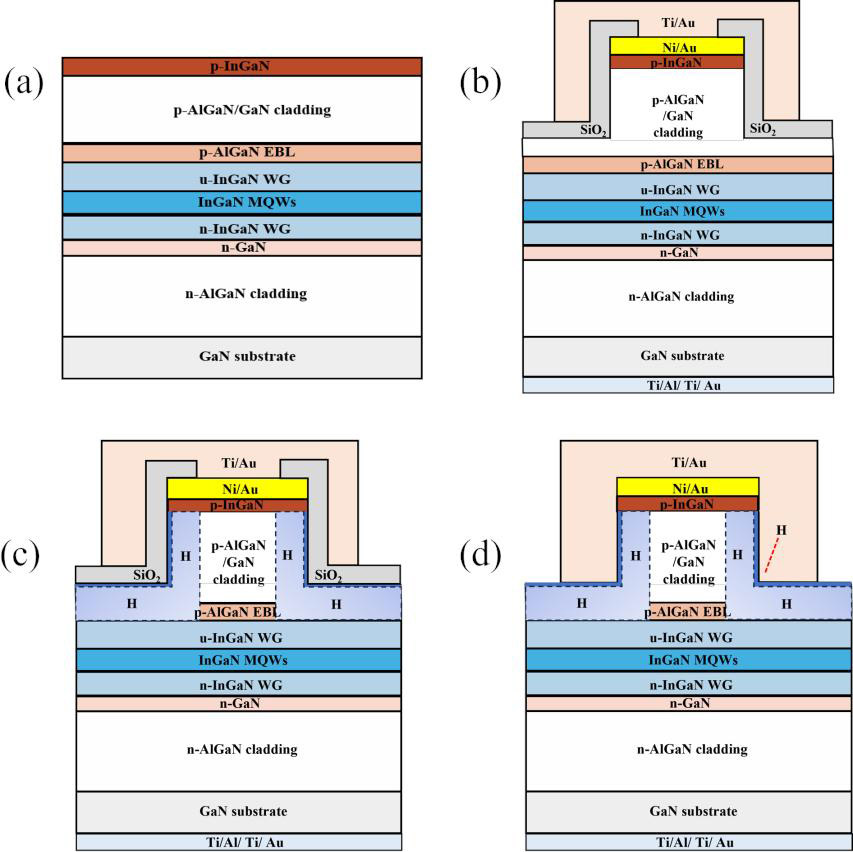
Figure 1: (a) GaN laser diode epitaxial structure. Further schematics of respective S1–S3 ridge laser diode passivation strategies: (b) conventional SiO2; (c) double-layer; and, (d) pure H-plasma laser diode.
The RF power was set at 2W with the inductively coupled plasma power at 300W. The gas supply was H and argon at rates of 30 and 5 standard cubic centimeters per minute (sccm), respectively. The plasma treatment was followed by 350°C rapid thermal annealing for 10 minutes.
The epitaxial structure was grown on c-plane freestanding GaN with the usual AlGaN cladding, and InGaN waveguide (WG) and multiple quantum well (MQW), layers, along with a p-AlGaN electron blocking layer (EBL) insertion below the p-cladding. The WG and cladding provide optical confinement, and the MQW generates and amplifies the photons via stimulated and spontaneous emission processes.
The ridge waveguide structure was 45μm wide and was created by etching down through the 130nm p-GaN contact layer and 440nm into the p-cladding.
The metal contact layers used nickel/gold (Ni/Au) for the p-electrode, and titanium/gold (Ti/Au) for the pad, applied after the passivation processes. The n-electrode/pad was a stack of Ti/Al/Ti/Au. The metal layers also provided reflectance of light back into the laser cavity.
The final laser diodes were separated into 1200μm-long cavities, and were treated to give 8%/98% reflectance for the front/rear facets, respectively.
In current-voltage measurements both H-plasma treated devices demonstrated a reverse-bias leakage current reduced by three orders of magnitude from ~10−5kA/cm2 for the conventional diodes to ~10−8kA/cm2 with H plasma treatment. The leakage with plasma treatment was close to the limit of the ability of the measurement equipment to register.
Under forward bias, the current injection at 6V was slightly lower in the pure plasma-treated diode, compared with the mixed passivation. The team suggests that this could be due to excessive hydrogen diffusion, adding: “In the future, the excess H entering the laser can be reduced by further optimizing the conditions (such as reducing the concentration of H gas, reducing the power of the ICP). In this way, only a small amount of H can form a complex reaction on the ridge, ensuring leakage and slope efficiency, and solving the voltage problem.”
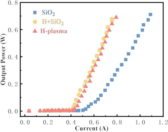
Figure 2: Light output power versus current for three device types.
The light output power of the diodes (Figure 2) showed a slope efficiency of ~1.95W/A of the plasma-treated devices over 1.40W/A with just SiO2 passivation. The pure H plasma diode (S3) had a slightly higher slope efficiency, compared with the mixed passivation device.
The researchers comment: “During the deposition process of SiO2 in S2, some minor diffusion of Si and O atoms may occur. However, in S3, no SiO2 was introduced, resulting in a lack of Si and O atom diffusion. The above results indicate that, compared to traditional SiO2 passivation layer, laser diodes treated with H plasma on the ridge exhibit significantly higher slope efficiency, demonstrating superior treatment effectiveness.”
By analyzing the theoretical factors that can contribute to the slope efficiency, the researchers believe that the primary effect of the H plasma treatment is to reduce the absorption coefficient of the p-GaN layers, decreasing the internal optical losses of the laser diodes.
Table 1: Summary of light output power-current behavior under three isolation/passivation conditions.
|
Isolation | Threshold current | Slope efficiency | Leakage |
| S1 | SiO2 | 0.55A | 1.40W/A | 10−5kA/cm2 |
| S2 | SiO2 + H plasma | 0.40A | 1.93W/A | 10−8kA/cm2 |
| S3 | H plasma | 0.42A | 1.96W/A | 10−8kA/cm2 |
The threshold current for the H-plasma-treated devices was around 0.4A, compared with 0.55A for the conventional laser diode (Table 1). The mixed device had a slightly lower threshold than the pure H plasma treatment of S3.
The emitted wavelengths of the devices were withing 1nm of each other: 450nm for S1 and S3, 449nm for S2. The researchers also studied the H plasma layer by secondary-ion mass spectroscopy (SIMS), finding the thickness to be 238nm. This is negligible in comparison to the 45μm ridge width.
Table 2: Benchmark of Suzhou et al’s results and other reports of blue laser diode performance.
Group |
Country | Report | Slope efficiency | Light output power | Threshold |
| Nippon Chemical Industrial | Japan | 2017 | 1.8W/A | 5W | — |
| Sony Corp | Japan | 2018 | 1.8W/A | 5.2W | — |
| Osram Group | Germany | 2014 | 1.6W/A | 4.5W | — |
| Osram Group | Germany | 2019 | 1.4W/A | — | 0.01A |
| Hiya/Nichia Corp | Japan | 2024 | 2W/A | — | 0.28A |
| Suzhou et al | China | 2024 | 1.96W/A | — | 0.42A |
The Suzhou et al team also provides some comparison data/benchmarks from previous research reports (Table 2).
https://doi.org/10.1364/OE.532577
The author Mike Cooke is a freelance technology journalist who has worked in the semiconductor and advanced technology sectors since 1997.


