


News: Optoelectronics
13 September 2024
Transfer-printed lasers on silicon photonics
Ireland’s Tyndall National Institute and Intel Corp in the USA report on a transfer printing method to apply indium phosphide (InP)-based epitaxial material to silicon-on-insulator (SOI) waveguides as a route to integrating O-band (1260–1360nm) lasers with silicon (Si) photonics circuits [Samir Ghosh et al, Appl. Phys. Lett., v125, p081104, 2024].
Target applications include data/telecoms, along with light distance and ranging (LiDAR), 5G telecoms, artificial intelligence (AI) and neuromorphic, programmable photonics, quantum computing, spectroscopy, and metrology.
The researchers see their approach as having potential for high-volume production over competing methods such as flip-chip integration, wafer bonding, and direct growth on silicon.
The team explains: “Transfer printing is an emerging technology for heterogeneous integration where massively parallel integration is a key attribute, which opens a path for high-volume manufacturability. It creates minimal waste of expensive epitaxial material, lowering the overall production cost and saving rare materials like indium.”
The lasers were fabricated after rather than before the transfer of III-V material to the silicon photonics wafer. This improved the alignment accuracy of the fabricated devices to the waveguide structures. The technique resulted in devices with a typical lasing threshold of 100mA at 20°C.
The integrated laser was built on top of 400nm silicon waveguides on 1μm buried oxide (BOx) (Figure 1). The researchers comment: “The thickness of the BOx layer is chosen to be as small as possible to achieve better heat dissipation through the silicon substrate.”
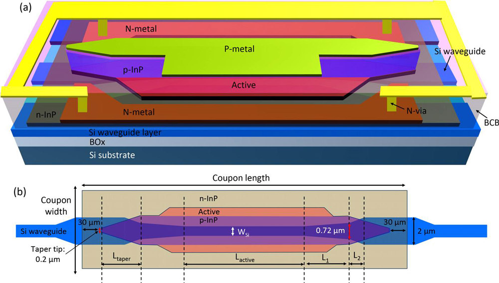
Figure 1: (a) Perspective view of integrated laser and (b) top-down view InP waveguide on silicon waveguide (only waveguide layers are shown for simplicity). Feedback structures (DBR grating or loop mirrors) and grating couplers are not shown.
The team designed adiabatic tapers of both the underlying silicon waveguide and InP laser structure to facilitate smooth light transfer by evanescent coupling. The silicon waveguide taper structure used two steps to ensure adiabatic power transfer between 2μm and 0.5μm without mode crossing.
The researchers designed three types of laser — Fabry–Pérot (FP), distributed Bragg reflector (DBR), and discrete mode laser (DML) — on the platform.
The FP lasers were realized using light mirror feedback loops from the outputs of a 1x2 multimode interference (MMI) coupler. A directional coupler tapped 12% of the power for external collection.
The DML used 200nm-deep slots etched into the silicon waveguide to provide mode selection. The slots were 306nm long, corresponding to an odd integer multiple of the quarter-wavelength of ~1310nm output. The team comments: “The main parameter here is the total number of slots with a higher number better to lower the threshold gain for a particular mode.”
The DBR laser used 24nm-deep etching to achieve a grating with a period of 210nm and 50% duty cycle. The reflectivity of the grating increased, in simulations, between 25% and 90%, as the number of periods increased from 150 to 500.
The waveguide widths in the active regions of the various structures were 600nm for the FP and DML, and 500nm for the DBR lasers.
The gain structure of the lasers was grown on 50mm InP substrates using metal-organic vapor phase epitaxy (MOVPE). The structure contained indium gallium arsenide (InGaAs) and indium aluminium arsenide (InAlAs) dual-release layers. The researchers explain: “This compound release layer approach reduces the undercut time considerably while providing a smooth surface for direct bonding.”
The epitaxial design included an 8-period multiple quantum well (MQW) active region.
The material was prepared into 1000μmx60μm ‘coupons’ which were released from the InP growth substrate and transfer printed onto the silicon waveguide target wafer. Before transfer the silicon waveguide surface underwent an oxygen plasma treatment. The coupon–SOI bond strength was tested by dipping in deionized water, and 95% of the coupons remained in place. This was the only yield loss during during the whole fabrication process.
Further fabrication included optical lithography of the process window, electron-beam lithography (EBL) of the laser, metalization of n-side of the devices, planarization with benzocyclobutene (BCB) polymer, p-side metalization, via-opening, bond-pad metalization, and etch removal of the dielectric layers from the gratings and loop mirrors (Figure 2).
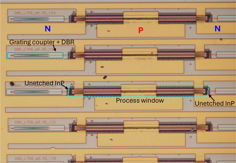
Figure 2: Optical microscopic image of few fabricated devices. All dielectric layers were cleared from grating coupler + DBR window.
EBL charging effects in the dielectric resist surface resulted in a 300nm alignment accuracy. This compares with a 500nm typical alignment accuracy for transfer printing of already fabricated lasers. Better alignment for the Tyndall/Intel method could be achieved by applying a thin conductive polymer coating on top of the EBL resist.
The FP and DM lasers were tested at room temperature in continuous wave (CW) operation (Figure 3). The free spectral range (FSR) between the FP peaks was about 110pm, corresponding well to the 2μm cavity length.
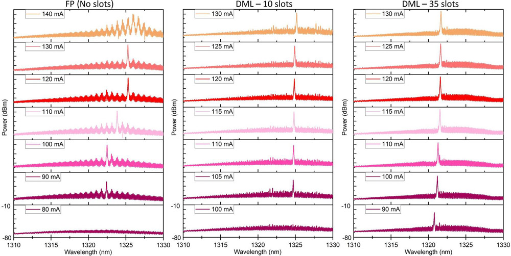
Figure 3: Measured spectra of FP and DM lasers for various bias currents at 20°C, plotted with 70dB vertical axis offset. Grating coupling loss is not subtracted.
For the DMLs the best side-mode suppression ratio (SMSR) was 35dB at 120mA current injection for the 35-slot device. The DML-35 slot wavelength shift rate due to current-induced heating was 0.01nm/mA. The 10 slot device showed mode hopping outside a linear single-mode regime.
The team reports on the 10-slot DML: “Mode-hop-free red shift is 0.42nm, which translates into a temperature tuning of 0.084nm/°C.”
The DML-10 delivered orders-of-magnitude lower power (10s of μW) than expected. This is attributed to silicon waveguide damage during fabrication with both grating coupler and feedback mirrors impacted by over-etching.
The DBR lasers showed a 170nm FSR, corresponding to a 1350μm cavity length (Figure 4). The best SMSR was 20dB. “Single-mode lasing with higher SMSR will be possible by incorporating narrowband mirror or high-Q resonator,” the researchers say.
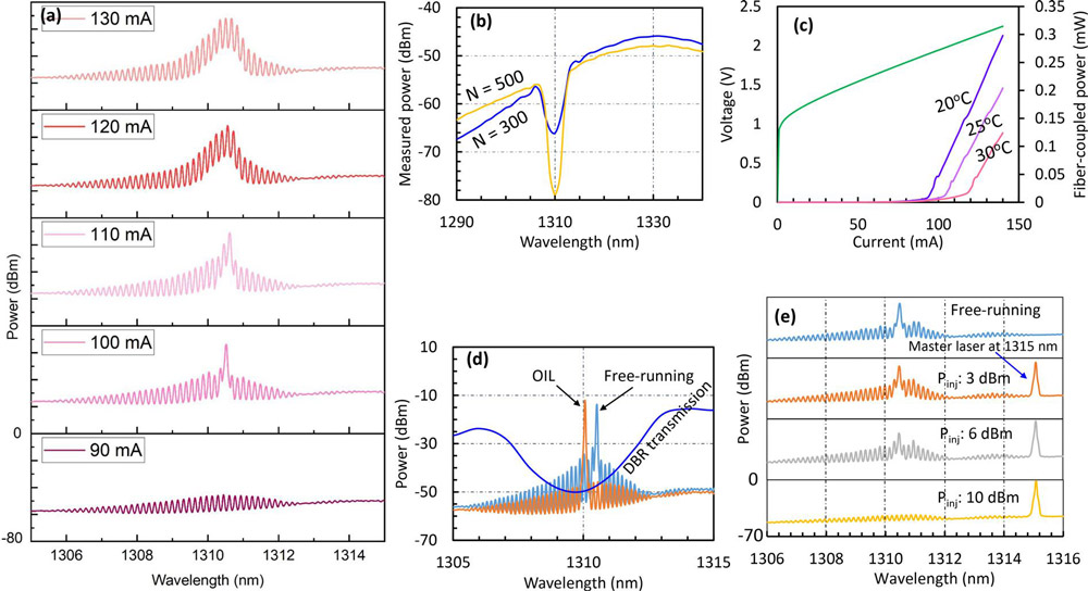
Figure 4: (a) DBR laser spectra with 200-pair front and 350-pair rear mirrors. (b) Transmission spectra for different N. (c) Light output-current-voltage curves. (d+e) Optical injection locking (OIL) experiments for (d) 1310nm-wavelength master laser and 100mA slave laser and (e) different levels of injected power (Pinj) at 1315nm-wavelength master laser, with slave at 110mA current.
Although the fiber-coupled output power was higher than for the DML-10 at 0.3mW, the researchers see this as low due to the same factors of silicon waveguide damage. This damage also increased the lasing threshold. The researchers estimate that the on-chip power could reach beyond 1mW at 100mA injection after compensating the −8db grating coupling loss.
The researchers recognize that data-centers require lasers that can operate beyond 80°C. They comment: “Our lasers have high-thermal impedance, which restricts their maximum operating temperature. A suitable path to improve temperature budget will be using a thermal shunt by connecting InP ridge to silicon substrate through a metal via. Alternatively, a thin layer of AlN or similar dielectric with high-thermal conductivity can be used as an intermediate layer between the coupon and SOI to dissipate the heat generated in the InP ridge.”
Transfer-printed lasers Silicon photonics InP SOI LiDAR
https://doi.org/10.1063/5.0223167
The author Mike Cooke is a freelance technology journalist who has worked in the semiconductor and advanced technology sectors since 1997.


