


News: Optoelectronics
5 September 2024
DBR-free thin-film InGaN VCSELs
University of Hong Kong, China, reports on a thin-film indium gallium nitride (InGaN) vertical-cavity surface-emitting laser (VCSEL) structure using high-contrast gratings (HCGs) rather than distributed Bragg reflectors (DBRs) to confine the vertical electromagnetic radiation modes [Wai Yuen Fu et al, Optics Letters, v49, p4505, 2024]. The researchers are hoping to improve lasing performance while reducing fabrication costs by omitting DBRs. A further simplification came through dropping the need for microdisk or implanted aperture structures to suppress lateral radiation modes.
The team explains: “Traditional laser diodes utilize pairs of DBRs or waveguiding layers, grown inside the epitaxy to form laser cavities—a process that can be cost-intensive.”
The researchers see future potential for photonic integrated circuit (PIC) and light detection and ranging (LiDAR) systems. InGaN-based laser systems are also key in optical storage (Blu-ray), high-resolution laser display technology, and visible light communication (VLC).
The researchers used a 440nm blue LED wafer, supplied by Enkris Semiconductor Inc, for the VCSEL fabrication process (Figure 1). Enkris produces its wafers by metal-organic chemical vapor deposition (MOCVD) on silicon (Si) substrates. The active light-generating region of the LED wafer consisted of 6 pairs of 5.9/7.0nm InGaN/GaN layers constituting a multiple quantum well (MQW) structure.
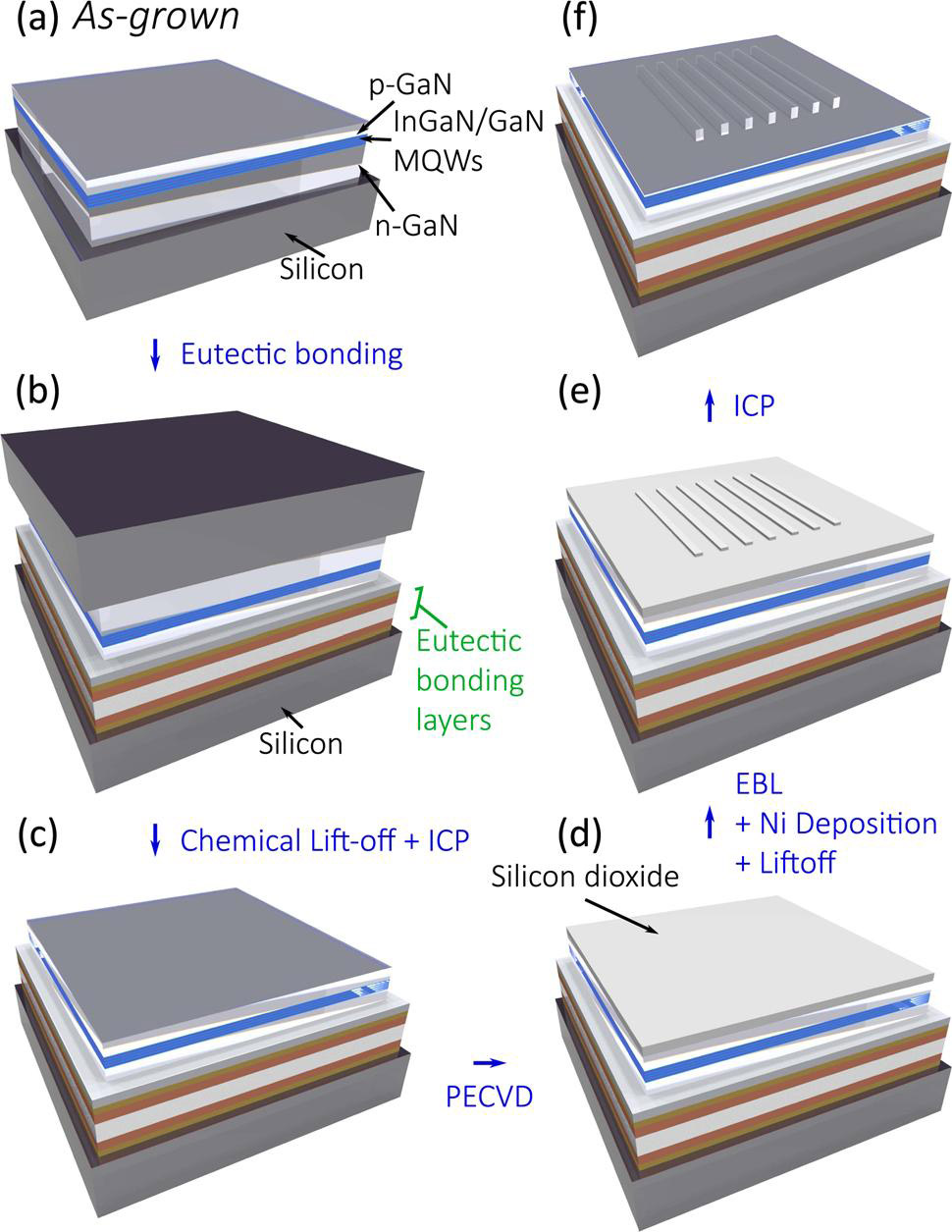
Figure 1: Process flow: (a) as-grown wafer; (b) eutectic bonding to silicon substrate; (c) silicon substrate removed by chemical lift-off and ICP; (d) PECVD oxide deposition; (e) grating patterning, Ni deposition followed by lift-off; (f) ICP etch of grating.
The fabrication began with electron-beam deposition of nickel/silver/nickel/gold (Ni/Ag/Ni/Au) on the p-GaN cap as a reflective metal layer. The wafer was then prepared for eutectic bonding to another silicon substrate with deposition of titanium/gold (Ti/Au) and electroplating of copper/tin (Cu/Sn) on the LED and target wafers. The eutectic bond was made through applying high pressure and temperature to the assembly.
The original substrate was removed using hydrofluoric acid chemical lift-off of the silicon, and inductively coupled plasma (ICP) etching of the GaN buffer and undoped GaN layers to a suitable thin-film thickness for the flipped VCSEL resonant cavity on the silicon handle wafer.
The grating (Figure 2) was formed in the n-GaN by ICP through a 30nm Ni mask and a plasma-enhanced chemical vapor deposition (PECVD) silicon dioxide pattern transfer layer. The Ni mask was patterned by electron-beam lithography (EBL). The grating region extended in a 20μmx20μm square. The grating depth was 250nm, and the period ~360nm. These choices were determined by intensive simulation work.
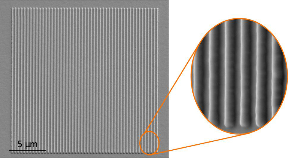
Figure 2: Scanning electron microscope (SEM) image of fabricated grating, with zoom-in circular inset.
The researchers report: “We refrained from any geometric shaping of the laser cavity, thus relying solely on the newly implemented top surface grating reflector and the existing bottom metallic reflecting layer without any DBR, using the thin-film GaN platform.”
The simulations suggested that there would be three relatively broad vertical reflection peaks reaching to almost 100% reflectivity in the wavelength range 400–460nm, around 407nm, 429nm and 449nm. The simulations also showed a couple of narrower peaks, representing laterally-propagating light. The researchers comment: “These lateral modes appear in the simulation due to the implementation of periodic boundary conditions and are not anticipated to occur in the actual device.”
The simulated peak separation suggested that the structure would be sufficient to suppress side-mode competition and to boost the quality factor (Q). Without the grating, a reflectivity around 17.8% was expected across the wavelength range.
With a 500nm cavity length between the bottom metallic layer and the top surface grating, the simulations suggested that a 432nm wavelength reflection with 73,000 Q-factor could be achieved. The 500nm cavity would also align the main resonance antinode with the active MQW region.
The fabricated structure was subjected to micro-photoluminescence measurements (μ-PL) with increasing excitation power from a 393.32nm 29.25ns/50kHz pulsed laser (Figure 3). The lasing peak was around 436nm, close to the 432nm simulation. The team attributes the minor discrepancy tentatively to the use of 2D instead of 3D simulations.
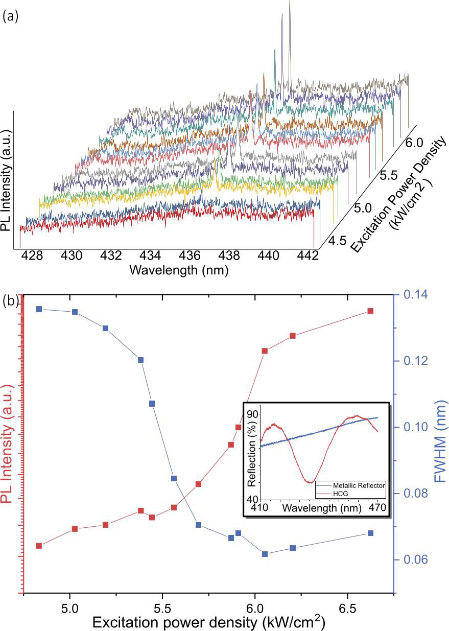
Figure 3: (a) Room-temperature μ-PL spectra (linear scale) for thin-film VCSEL under increasing excitation power density. (b) Corresponding plots displaying linewidths (linear) in blue and integrated PL intensities (log scale). Inset shows reflection spectra of bottom metallic reflector and HCG, measured under normal incidence from top side.
The laser threshold was around 5.5kW/cm2 power density. The measured Q-factor was 4600. In regions without the grating there was no lasing up to 30kW/cm2 excitation, when the power density began to physically damage the thin-film material.
Despite the absence of lateral confinement structures such as etched micro disks or implanted apertures, the lateral resonance modes were effectively suppressed, giving vertical-cavity laser emissions.
The researchers comment: “Although the demonstrated lasing threshold of 5.5kW/cm2 marks an improvement over earlier studies on InGaN-based VCSELs, which reported thresholds exceeding 100kW/cm2, it understandably does not yet match the performance of state-of-the-art VCSELs equipped with refined DBRs that typically lase at well below 100W/cm2. However, the successful demonstration of room-temperature lasing under optical pumping conditions confirms the feasibility of the VCSEL operation without DBRs, providing a low-cost solution for lasing devices.”
The team hopes that optimization of the HCG reflector will result in competitively reduced thresholds with a more economical fabrication process than DBR-based VCSELs.
DBR-free thin-film InGaN VCSELs InGaN VCSELs MOCVD PECVD ICP
https://doi.org/10.1364/OL.534465
The author Mike Cooke is a freelance technology journalist who has worked in the semiconductor and advanced technology sectors since 1997.


