News: Microelectronics
3 April 2025
Enhancing GaN diode performance with p-oxides
École Polytechnique Fédérale de Lausanne (EPFL) in Switzerland has reported significant improvement in p-oxide/gallium nitride (GaN) heterojunction (HJ) PiN bipolar diodes by inserting a crystalline p-type lithium-doped nickel oxide (p-LiNiO) layer between the drift layer and high-hole-density p-type amorphous nickel oxide layer [Zheng Hao et al, IEEE Electron Device Letters,published online 7 March 2025]. The full device achieved 1.7V turn-on (VON), low 1.15mΩ-cm2 specific on-state resistance (RON,sp), and high 1065V breakdown voltage (BV).
The team reports comparable performance to GaN homojunction PiN diodes but with simpler fabrication and greater design flexibility. The researchers comment: “Our findings show the potential of p-NiO/LiNiO to replace p-GaN for effective localized p-doped regions in GaN power devices.”
Homojunction GaN devices are usually processed by metal-organic chemical vapor deposition (MOCVD) with the p-type layers doped with magnesium. Unfortunately, the doping has a high activation energy and is difficult to activate effectively, resulting in low hole concentrations.
The researchers comment: “Developing highly conductive and high-quality p-layers that can be deposited with great flexibility is crucial to enable advanced device concepts, such as junction barrier Schottky (JBS) diodes, ring terminations, field plates, among others.”
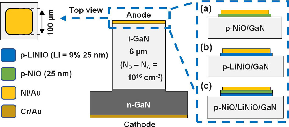
The vertical p-NiO heterojunction diode structures on the same GaN chip with three combinations of p-NiO and p-LiNiO as p-region (Figure 1). The anode and cathode metal electrodes were nickel/gold (Ni/Au) and chromium/gold (Cr/Au), respectively. The intrinsic GaN (i-GaN) drift layer was 6μm thick. Patterning was supplied by a 300nm silicon dioxide hard mask.

Figure 1: Three p-(Li)NiO/GaN heterojunction diodes schemes: (a) p-NiO (25nm), (b) p-LiNiO (25nm), and (c) p-NiO/LiNiO (25nm/25nm) — p-type regions deposited and patterned on the GaN surface.
The p-LiNiO was applied using 400°C pulsed laser deposition (PLD) on a LiNiO target with 9% Li content. The target was ablated using a 248nm krypton fluoride (KrF) excimer laser. The p-NiO deposition was by room-temperature RF sputtering. The 2μm cathode n-GaN and i-GaN drift layers were deposited by MOCVD on 2-inch freestanding GaN from Enkris Semiconductor Inc. A 6.3μm-deep mesa etch was used to isolate the devices. A Schottky barrier diode (SBD) reference was created by depositing the anode metals directly on the i-GaN drift layer.
In pre-fabrication material characterization, the researchers demonstrated p-NiO layers with Hall carrier concentration and mobilities of 2x10¹⁹/cm3 and 0.3cm2/V-s, respectively. The resulting resistivity was 0.94Ω-cm. The team comments: “It is worth noticing that although the hole mobility in p-NiO is lower than in p-GaN, this is not relevant for applications where the p-layers are not aimed for conducting current, but for band-structure engineering. This is the case in localized p-pockets for junction termination extensions and electric field management, as well as in achieving enhancement mode in lateral devices, for which the high hole concentration is a more important feature.”
The resistivity of p-LiNiO was much larger at 5kΩ-cm. The researchers suggest the carrier density was of order 1015–1017/cm3, based on an expected mobility in the range 0.01–1cm2/V-s. X-ray analysis showed the p-LiNiO to be crystalline, while the p-NiO was amorphous.
The researchers proposed the p-NiO/p-LiNiO structure as effectively combining high hole concentration in the p-NiO with superior p-LiNiO film quality. The team explains: “This approach compensates for the poor quality of sputtered p-NiO while retaining a high hole density, thereby improving the p-n heterojunction performance.”
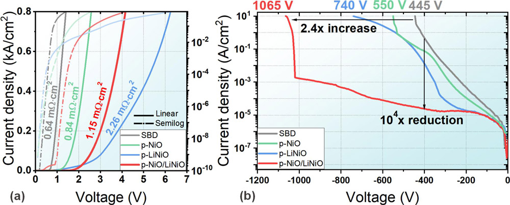
The p-NiO/LiNiO diode structure enabled (Figure 2) a high hole density injected from the p-NiO layer through the high film quality of p-LiNiO, achieving small RON,sp with more than 1000V high BV.

Figure 2: (a) Forward and (b) reverse current–voltage (I–V) curves measured from p-(Li)NiO/GaN heterojunction diodes and reference SBD.
The p-NiO/p-LiNiO bipolar diode was found to combine a relatively low on-resistance with more than 1000V BV (Table 1). The researchers comment: “Compared to the large VON (>3V) in regular GaN homojunction PiN diodes, the smaller VON (1.7V) of p-NiO/LiNiO-GaN heterojunction PiN diode is advantageous for reducing conduction losses. Additionally, double-sweep I–V characteristics performed on the p-NiO/LiNiO-GaN diode showed negligible hysteresis leading to a stable switching operation.”
Table 1: Characteristics of EPFL variant diode structures.
Device |
VON | RON,sp | BV |
| SBD | 0.7V | 0.64mΩ-cm2 | 445V |
| p-NiO | 1.1V | 0.84mΩ-cm2 | 550V |
| p-LiNiO | 1.0V | 2.26mΩ-cm2 | 740V |
| p-NiO/p-LiNiO | 1.7V | 1.15mΩ-cm2 | 1065V |
The team attributes the higher BV for the p-NiO/LiNiO-GaN diode to lower defect level in the heterojunction from the crystalline epitaxial p-LiNiO layer inserted between the high-hole-concentration p-NiO and GaN drift layer, increasing the electron tunneling barrier and reducing leakage.
Table 2: Comparison of EPFL p-NiO/LiNiO-GaN HJ PiN diode to other reported GaN PiN diodes.
Institution & year |
VON | RON,sp | BV | Diode type |
| Nagoya Univ. 19 | ~3.2V | 1.2mΩ-cm2 | 905V | p-GaN epi |
| Virginia Tech. 23 | ~3V | 0.8mΩ-cm2 | 1700V | p-GaN epi |
| Cornell 16 | ~3V | 0.55mΩ-cm2 | 1700V | p-GaN epi |
| ASU 19 | ~3V | 0.8mΩ-cm2 | 1270V | p-GaN regrowth |
| Cornell 17 | >3.2V | 3.9mΩ-cm2 | 1136V | p-GaN regrowth |
| EPFL 21 | 1.6V | 1.6mΩ-cm2 | 387V | p-oxide |
| NPU 21 | 2.3V | 1.42mΩ-cm2 | 350V | p-oxide |
| Latest EPFL work 25 | 1.7V | 1.15mΩ-cm2 | 1065V | p-oxide |
The researchers also compare their diodes with other reports (Table 2), showing their latest “p-NiO/LiNiO-GaN heterojunction PiN diode achieves competitive RON,sp and BV values comparable to GaN homojunction PiN diodes, and larger BV compared to other p-oxide/GaN HJ PiN diodes.”
GaN Heterojunction PiN bipolar diodes P-oxides MOCVD
https://doi.org/10.1109/LED.2025.3549252
The author Mike Cooke is a freelance technology journalist who has worked in the semiconductor and advanced technology sectors since 1997.


