


News: Microelectronics
17 April 2025
RISC processor based on 2D semiconductor FETs
Fudan University and Shaoxin Laboratory in China have reported “one of the most complex functional circuits based on 2D semiconductors to date”, consisting of 5900 molybdenum disulfide (MoS2) field-effect transistors (FETs) combined into a RISC-V 32-bit reduced instruction set computer [Mingrui Ao et al, Nature, published 2 April 2025].
The researchers see their basic two-dimensional (2D) MoS2 transistor structure as competitive and well aligned with the 2022 IEEE International Roadmap for Devices and Systems (IRDS) targets.
The team comments on future prospects: “Silicon integrated circuit designs are well established, but they may not be adaptable to emerging fields such as edge computing and intelligent sensing, where 2D semiconductors are expected to excel.”
Edge computing refers to distributed computing models where computation is performed closer to the data source, somewhat like reflex responses not needing a stimulus signal to reach the brain before eliciting a reaction.
In addition to the RV32-WUJI RISC-V 32-bit microprocessor, the team has developed 25 logic units for a complete standard cell library. It may or may not be relevant but wuji is a concept in Chinese philosophy meaning variously and tentatively “ultimateless”, “limitless”, “the ultimate of nothingness”, and “non-polar” (“wu”/無 = “nothingness”, “ji”/極 = “pole”).
The researchers comment: “The architecture of this arithmetic logic unit with a 32-bit serial data path was designed to reduce static power consumption and hardware overhead to address power efficiency and cost concerns rather than performance requirements, thereby making it suitable for use in scenarios such as edge-embedded environments for small Internet of Things devices.”
The microprocessor integrated circuit consisted of 5900 MoS2 FETs and a maximum logic path of 17 stages of cascaded logic elements positioned between flip-flops. The supply voltage was 4V. The interconnection of the transistors was through 4 connect layers: the source, drain, gate (M0); logic (M1); and module (M2–3).
The three-atom-thick MoS2 for the FETs was deposited on 4-inch insulating sapphire substrate. The sources for the MoS2 was a sponge-like mix of molybdenum oxide (MoO3) and graphene oxide, and sulfur. The sponge and sulfur precursors were heated to 700°C and 220°C, respectively, in a 200mm-diameter quartz tube furnace and deposited on an inverted sapphire substrate for 15 minutes at 0.02Pa pressure. Shenzhen Six Carbon Technology Inc supplied most of the MoS2/sapphire substrates used by the team.
The sapphire insulation provided complete isolation of the individual transistors making up the RV32-WUJI processor. The researchers liken the use of the sapphire substrate to the silicon-on-insulator technology used in present-day advanced silicon electronics, aiming to reduce parasitic capacitance and current leakage.
The team adds: “The MoS2 channel is only three atoms thick and is free of dangling bonds in the plane, making it more favorable for electrostatic control in a planar transistor structure.”
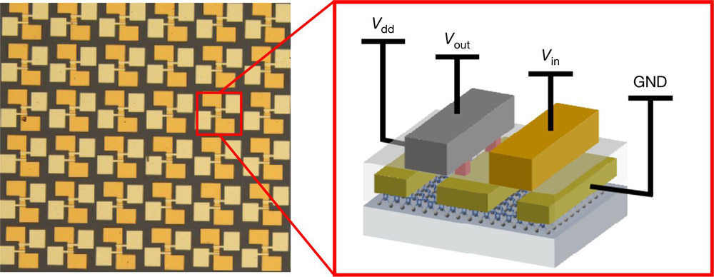
Figure 1: Transistor scheme for enhancement- and-depletion-mode inverter.
The basic unit of the RV32-WUJI was top-gate n-type metal–oxide–semiconductor (MOS) FETs (Figure 1). The use of ion implantation to control the threshold voltage (VTH), as in conventional silicon electronics, is excluded for atom-level transistors such as MoS2 FETs, so alternative strategies had to be implemented.
In the RV32-WUJI the threshold was controlled by using different gate metals, aluminium (Al, load) or gold (Au, drive), and by seeding-layer optimization of the high-k dielectric insulation between the metal gate and MoS2 channel. The researchers comment: “Such combined strategies can efficiently tune the VTH of MoS2 FETs for circuit-level matching and optimization in M1 and the gate layer.”
The dielectric gate insulation/passivation was seeded with 1nm amorphous silicon dioxide on which 15nm of high-k hafnium oxide was grown by atomic layer deposition.
Wafer-scale fabrication posed many challenges, considering the delicate nature of the basic transistor. The team adopted systematic co-optimization along with machine learning methods to meet the device performance needed for high wafer-level transistor yields of 99.92%. The inverter yield was 99.77%.
The researchers comment: “Inverters are the basis of all logic units. Based on the above inverter characteristics, we built a 2D process design kit with a complete basic logic-unit library.”
Of course, as the complexity of the circuits increased, yields decreased, falling to 7% for a 64-bit register with 1152 transistors. The team writes: “This can reasonably be attributed to factors such as the relatively low grade of the cleanroom in our laboratory (compared to an industrial-grade cleanroom) and the stability of the processing tools used. It is, therefore, necessary to further optimize and improve the manufacturing process of VLSI 2D integrated circuits in a more industrial manner.”
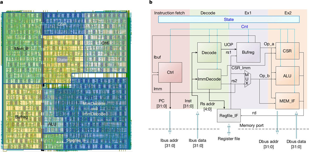
Figure 2: a, RV32-WUJI core architecture with nine basic modules. b, Schematic data path.
The final RV32-WUJI chip (Figure 2) consisted of a 1-bit arithmetic logic unit (ALU) for performing operations, a control status register module (CSR), an instruction-decoding module, an immediate-number-decoding module and a control module (Ctrl) with the program counter. Intermediate results were stored in a buffer register, and a small state machine monitored instruction execution. Interface modules connected memory and register sections.
The researchers performed a sequence of operations, “1946+25=1971”, and then “1971+53=2025” at 1kHz clock rate with0.43mW power consumption. The team explains the significance of these figures: “Here, 1946 and 1971 represent the years in which ENIAC (the first general-purpose programmable electronic digital computer) and the Intel 4004 (the first commercially produced silicon microprocessor) were created.”
The researchers used n-type transistors with relatively long 3μm channel lengths, rather than the complementary p/n-type structure favored in mainstream electronics. The use of just n-type transistors impacted dynamic performance and power consumption of the MoS2 FETs, compared with CMOS.
The team comments: “A more suitable circuit architecture, such as pass-transistor logic, may be a compromise solution for circuits using single-polarity transistors. In the long run, we anticipate that further optimization and innovation in processing and materials will facilitate the realization of 2D CMOS in the short-channel regime. By then, the full potential of 2D semiconductors will be unlocked.”
https://doi.org/10.1038/s41586-025-08759-9
https://en.wikipedia.org/wiki/Wuji_(philosophy)
https://www.6carbon.com/index-en.php
The author Mike Cooke is a freelance technology journalist who has worked in the semiconductor and advanced technology sectors since 1997.


