


News: Microelectronics
10 April 2025
GaN HEMT hits 85.2% PAE record at 2.45GHz
Japan-based Fujitsu Ltd has reported gallium nitride (GaN) high-electron-mobility transistors (HEMTs) on free-standing GaN substrates operating at 2.45GHz in the industrial, scientific & medical (ISM, 2.4–2.5GHz) reserved band with 85.2% power-added efficiency (PAE) and 89.0% drain efficiency (DE) [Toshihiro Ohki et al, Appl. Phys. Express, p18, p034004, 2025].
The team reports: “To the best of our knowledge, our device sets a new record for the highest power-added efficiency and drain efficiency among discrete GaN HEMTs, highlighting the superior potential of GaN-on-GaN HEMTs for highly efficient RF power amplifiers.” Fujitsu had also claimed the previous record set in 2021 of 82.8% PAE at 2.45GHz.
The researchers believe the methods used to boost efficiency could benefit performance at other frequencies, even in the 100GHz sub-terahertz range. The team particularly focused on reducing silicon and carbon contamination on the substrate surface and in the channel regions, respectively, which have delayed expected performance benefits of using free-standing GaN substrates.
The researchers explain: “GaN-based HEMTs on free-standing GaN substrates (GaN-on-GaN HEMTs) can effectively suppress electron trapping at crystal defects during high-frequency and high-power operation, owing to their low dislocation density and the elimination of nucleation layers through homoepitaxy.”
GaN HEMTs are widely used in wireless communications and radar systems, and more recently for power conversion applications, including for electric vehicles.
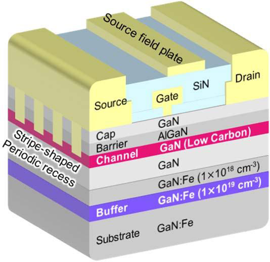 Figure 1: Schematic of GaN-based HEMT on free-standing GaN substrate.
The researchers grew the epitaxial material for the HEMTs (Figure 1) on 4-inch free-standing semi-insulating GaN through metal-organic vapor phase epitaxy (MOVPE). The GaN substrate had a dislocation density less than 5x10⁶/cm3. Before the epitaxy, silicon (Si) residue was removed from the substrate surface by a hydrofluoric acid pre-treatment. The trace Si level was reduced by two orders of magnitude with the aim of reducing lateral leakage currents at the epi/substrate interface in the final HEMT devices.
The initial iron (Fe)-doped GaN layers were further features designed to reduce leakage currents, ensuring high power-added efficiency.
The channel layer was grown with a view to reducing the carbon content, which was achieved by increasing the V/III ratio from 1600 to 8200. The higher ratio increase reduced the relative carbon-containing group-III metal-organic concentration in the precursor mix. The effectiveness of this strategy was evidenced by a photoluminescence study, which showed yellow luminescence associated with carbon incorporation decreasing by a factor of 0.075 by increasing the V/III ratio.
The HEMT epitaxy was completed with a 31% aluminium (Al)-content AlGaN barrier, and GaN cap.
The fabricated HEMTs had ohmic source and drain electrodes that used periodically etched recesses that allowed the metals direct contact with the channel layer. The source/drain metals were annealed titanium/aluminium. The contact resistance was thus reduced from 0.38Ω-mm to 0.25Ω-mm.
The team comments: “This structure provides a more stable lower contact resistance than a planar-type recessed structure because the electrodes contact the 2DEG directly without an intervening barrier layer and because a thin barrier layer is not required, preventing reduction in the 2DEG beneath the electrodes. Furthermore, the stripe-shaped recess structure also reduces the thermal budget, which can be an origin of electron traps, compared with a process involving a regrowth layer made of highly Si-doped GaN.”
The 0.5μm-long gate consisted of nickel/gold. Passivation was provided by plasma-enhanced CVD silicon nitride (SiN). The HEMT design also included source and gate field plates.
Three-terminal DC studies showed 390Ω/□ sheet resistance of the two-dimensional electron gas (2DEG) channel, 853mA/mm maximum drain current, and 4.74Ω-mm on-resistance with +2V gate potential. At 10V drain bias, the maximum transconductance and threshold voltage were 288mS/mm and −1.77V, respectively.
Load-pull measurements in the 2.45GHz ISM band gave cut-off frequency (fT) and maximum oscillation frequency (fmax) of 11.5GHz and 20.3GHz, respectively, with 55V drain bias, and 10mA drain current. The total gate periphery Wg was 3.2mm (10x320μm).
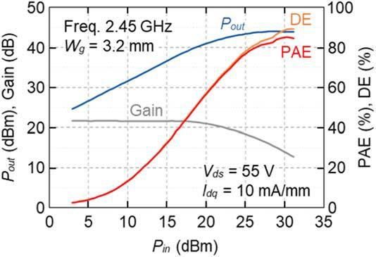
Figure 2: Input–output power (Pin–Pout) characteristics of GaN-on-GaN HEMT at 2.45GHz with fundamental and harmonic impedance set to PAE-matching conditions.
A 85.2% maximum PAE and 89.0% drain efficiency were extracted from input–output power measurements (Figure 2). The peak 44.04dBm output power corresponds to a power density of 7.9W/mm.
The researchers comment: “These results surpass those of previous reports and are attributable to both the reduction in electron-trapping phenomena through improved channel quality and the suppression of substrate-side leakage current via a reduction in residual silicon at the sub/epi interface during high-power operation.”
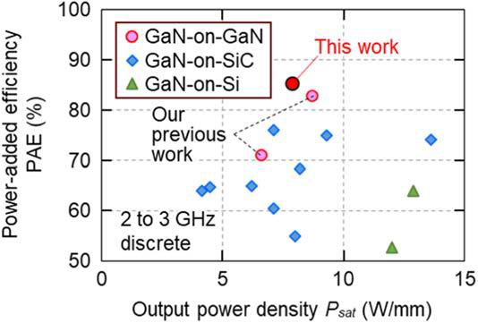
Figure 3: Comparison of load-pull measurement results of discrete GaN-based HEMTs in 2.45GHz ISM band.
The researchers also present a benchmark plot comparing their load-pull results with discrete GaN-based HEMTs reported in a frequency range of 2–3GHz (Figure 3).
https://doi.org/10.35848/1882-0786/adbc79
The author Mike Cooke is a freelance technology journalist who has worked in the semiconductor and advanced technology sectors since 1997.


