


News: Microelectronics
14 April 2025
Infineon launches first industrial GaN transistor product family with integrated Schottky diode
Infineon Technologies AG of Munich, Germany has launched what it says are the first gallium nitride (GaN) power transistors with integrated Schottky diode for industrial use. The product family of medium-voltage CoolGaN Transistors G5 with integrated Schottky diode increases the performance of power systems by reducing undesired deadtime losses, further increasing overall system efficiency. Additionally, the integrated solution simplifies the power-stage design and reduces bill-of-materials (BOM) cost.
In hard-switching applications, GaN-based topologies may incur higher power losses due to the larger effective body diode voltage (VSD) of GaN devices. This gets worse with long controller dead-times, resulting in lower efficiency than targeted. Until now, power design engineers often require an external Schottky diode in parallel with the GaN transistor or try to reduce dead-times via their controllers. All of which is extra effort, time and cost. The new CoolGaN Transistor G5 is said to significantly reduce these challenges by offering a GaN transistor with an integrated Schottky diode appropriate for use in server and telecom intermediate bus converters (IBCs), DC–DC converters, synchronous rectifiers for USB-C battery chargers, high-power power supply units (PSUs), and motor drives.
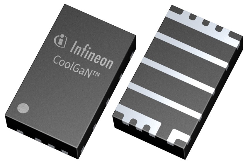
Picture: Infineon’s CoolGaN Transistors with integrated Schottky diode.
“As gallium nitride technology becomes increasingly widespread in power designs, Infineon recognizes the need for continuous improvement and enhancement to meet the evolving demands of customers,” says Antoine Jalabert, VP of Infineon’s Medium-Voltage GaN product line, “The CoolGaN Transistor G5 with Schottky diode exemplifies Infineon’s dedication to an accelerated innovation-to-customer approach to further push the boundaries of what is possible with wide-bandgap semiconductor materials.”
GaN transistor reverse conduction voltage (VRC) is dependent on the threshold voltage (VTH) and the OFF-state gate bias (VGS) due to the lack of a body diode. Moreover, the VTH of a GaN transistor is typically higher than the turn-on voltage of a silicon diode, leading to a disadvantage during the reverse conduction operation (third quadrant). Hence, with this new CoolGaN Transistor, reverse conduction losses are lower. Also, due to compatibility with a wider range of high-side gate drivers, and with deadtime relaxed, there is broader controller compatibility, resulting in simpler design.
The first of several GaN transistors with integrated Schottky diode is the 100V 1.5mΩ transistor in a 3mm x 5mm PQFN package. Engineering samples and target datasheet are available upon request.
Infineon launches CoolGaN G3 Transistor in new silicon-footprint packages
Infineon launches CoolGaN transistor families built on 8-inch foundry processes


