


News: Microelectronics
25 April 2025
Atomic layer etch surface treatment for AlGaN Schottky barrier diodes
Saudi Arabia’s King Abdullah University of Science and Technology (KAUST) reports on using atomic layer etching (ALE) to improve the performance of aluminium-rich III-nitride (III-N) Schottky barrier diodes (SBDs) [Tingang Liu et al, Appl. Phys. Lett., v126, p152109, 2025]. In particular, SBDs fabricated using ALE demonstrated breakdown voltages of 1205V, compared with just 308V for SBDs processed without ALE.
The team comments: “By reducing interface traps and eliminating native oxide, ALE leads to lower leakage current and a more uniform Schottky barrier.”
Compared with metals like gallium (Ga), aluminium (Al) has a faster oxidation rate, giving aluminium pots and pans a rather dull finish. AlGaN semiconductor metal-organic chemical vapor deposition (MOCVD) epitaxial structures frequently use a GaN cap layer to protect the underlying material from oxidation.
The KAUST team explains: “In AlGaN materials, the native oxide is typically around 1–3nm thick. The excess oxide layer is likely due to a high density of defects, which makes the surface more susceptible to oxidation. The defective surface layer forms at the end of the MOCVD growth process during chamber cool-down, where residual MO sources in the chamber contribute to its continuous growth at a lower temperature.”
The defective layer tends to encourage unwanted oxidation during processes such as the rapid thermal annealing of metal contacts. The ALE process reduces surface defectivity, reducing oxidation in later fabrication steps. The ALE also removes any native oxide that forms on the Al-rich materials on exposure to air.
By removing these layers, the KAUST team hopes to show the way to “enhancing the performance and reliability of AlGaN-based power devices for next-generation high-voltage applications”.
The researchers describe the benefits: “Atomic layer etching (ALE) technology is an etching strategy that removes materials with atomic accuracy. Unlike conventional reactive ion etching (RIE), which normally operates with high RF power (usually over 300W), plasma ALE usually gently removes materials with low ion energy (~10eV) after a specific chemical treatment at a low speed. The self-limited process allows ALE to achieve precise thickness control and minimal surface damage.”
Increasing the Al-content of the III-N semiconductor material should increase the bandgap from the 3.4eV of GaN nearer to the 6.2eV of AlN. A wider bandgap is associated with a higher critical electric field for breakdown, which should allow high voltages to be reached in smaller structures, as needed in power-handling devices. By mitigating surface defects, ALE could advance performance in other power device types such as field-effect transistors and p-n diodes.
The researchers used 2-inch AlN/sapphire templates to grow 500nm epitaxial 1300°C AlN, followed by 200nm 1150°C silicon-doped Al0.86Ga0.14N, both through MOCVD. The AlN template layer was 1μm thick. The screw- and edge-dislocation densities in the epitaxial layers were estimated to be 2.79x10⁷ and 3.41x10⁸/cm2, respectively, based on x-ray analysis.
The team fabricated its SBDs (Figure 1) on 1cm x 1cm pieces cut from the epitaxial material by laser. Before fabrication, the pieces were cleaned in a sulfuric acid/hydrogen peroxide ‘piranha’ solution and in a buffered oxide etchant consisting of hydrofluoric acid and ammonium fluoride (NH4F) solutions.
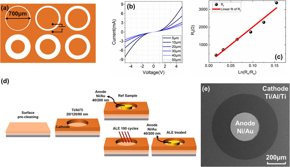
Figure 1: (a) Schematic view of CTLM patterns. (b) and (c) CTLM measurement results and linear fit for contact resistivity calculation. (d) Fabrication processes of reference and ALE-treated samples; red arrows show position of treatment. (e) Scanning electron microscope (SEM) view of fabricated device.
The team explains: “These cleaning steps were employed to eliminate impurities generated during laser cutting and to remove most contamination present on the sample surfaces.”
To assess the contact resistivity of the ohmic contacts circular transmission line measurement (CTLM) structures were fabricated, using patterned and annealed sputtered titanium/aluminium/titanium (Ti/Al/Ti) metal stacks. The contact resistivity was estimated at 2.01x10⁵Ω-cm2. Hall measurement showed the AlGaN layer to have sheet resistance, carrier concentration, and mobility of 421kΩ/□, 4.3x10¹⁶/cm3, and 17.4cm2/V-s, respectively.
The ohmic metal cathode of the SBDs was the same as used in the CTLM structures. The nickel/gold Schottky anode was deposited with or without ALE. The SBD without ALE served as a reference sample. The Schottky metals were deposited by electron-beam evaporation.
The ALE was carried out using equipment from Oxford Instruments. The etch cycle consisted of a chlorine dose (0.03s), followed by a purge (10s), etch (5s), and spacer (0.4s). The cycle was repeated 100 times, to give an estimated etch depth of 10nm, based on atomic force microscope (AFM) measurements. The SBD featured 300μm-diameter anode and 200μm gap distance to the cathode.
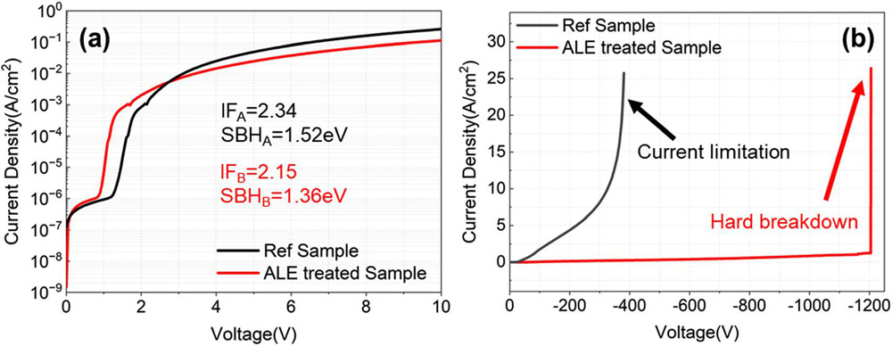
Figure 2: (a) Forward and (b) reverse current–voltage (I–V) characteristics of reference and ALE-treated samples.
The on/off current ratio of the ALE SBD and reference was 106 for both (Figure 2). The measurement points were 10V on and −5V off. The ideality for the ALE SBD was 2.15, compared with 2.34 for the reference. The Schottky barrier heights were 1.36eV and 1.52eV for the ALE and reference SBDs, respectively. Capacitance–voltage (C–V) measurements gave higher barrier heights of 4.85eV for ALE samples and 5.05eV for the reference.
The researchers comment: “The discrepancy between the C–V SBH and I–V SBH probably arises from the high density of interface states in the surface oxide layer of the Ref sample and plasma-chemical process-induced interface states at the surface of the ALE-treated sample, respectively. ALE improved the ideality factor of SBDs but resulted in a slightly decreased Schottky barrier height.”
The breakdown characteristics of the devices were significantly different at 308V for the reference and 1205V for the ALE SBD. Also, the breakdown mode was different: the reference broke the leakage current limitation, while the ALE SBD underwent sudden hard breakdown.
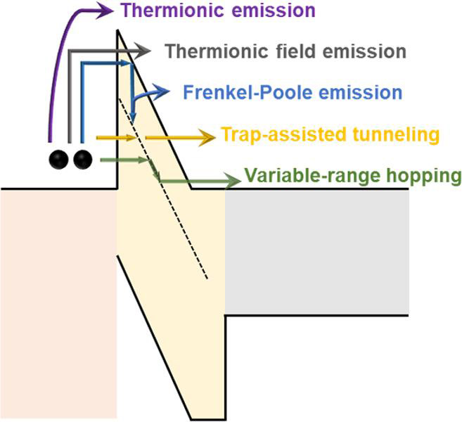
Figure 3: Current flow and breakdown mechanisms through Schottky barrier.
The researchers used temperature-dependent measurements to analyze the current leakage and breakdown mechanisms (Figure 3). Although the ALE SBD had improved reverse-bias performance over the reference, the leakage current magnitude was too high for it to be attributed to thermionic or thermionic field emission effects. Rather than these conventional electrode-limited conduction mechanisms, the team suggests that defect-assisted conduction is to blame for carriers sneaking through the barrier through trap-assisted tunneling (TAT) or variable range hopping (VRH). The temperature analysis suggested that TAT was less of a factor in the ALE SBD compared with the reference. The VRH component was thought to be comparable in both device types. The team concludes that the ALE treatment mainly improved the high-field carrier transport performance.
Atomic layer etch AlGaN Schottky barrier diodes AlGaN MOCVD
https://doi.org/10.1063/5.0251499
The author Mike Cooke is a freelance technology journalist who has worked in the semiconductor and advanced technology sectors since 1997.


