


News: Microelectronics
28 April 2025
Novel Crystal Technology boosts gallium oxide MOSFET power figure of merit record by 3.2-fold
Novel Crystal Technology Inc (NCT) of Saitama, Japan has developed a gallium oxide vertical MOS transistor (β-Ga2O3 MOSFET) with a record power figure of merit (PFOM, VBR2/Ron,SP) of 1.23GW/cm2, 3.2 times higher than the previous record (presented at the 72nd Japan Society of Applied Physics (JSAP) Spring Meeting 2025 on 15 March).
Overview
Wide-bandgap semiconductor materials such as silicon carbide (SiC) and gallium nitride (GaN) are being developed to replace silicon power devices. However, gallium oxide (β- Ga2O3) has superior material properties, and cost is more competitive due to the faster crystal growth speed. Because of its low-loss and low-cost characteristics, it is expected to be applied to various power electronic devices such as home appliances, industrial equipment, electric vehicles, trains, solar power generation, and wind power generation. R&D on Ga2O3 is hence accelerating at both companies and research institutes worldwide, in order to reduce the size and efficiency of electrical equipment.
NCT has been working on commercializing β-Ga2O3 MOSFETs under the ‘Research and Development of 10kV Class Gallium Oxide Trench MOSFETs’ and ‘Research and Development of Inversion-type channel Gallium Oxide MOS Transistors’ programs of the National Security Technology Research Promotion Fund (JP004596) since being awarded a contract by Japan’s Acquisition, Technology and Logistics Agency (ATLA) in 2019.
The record PFOM of 1.23GW/cm2 was achieved by incorporating a high-resistance guard ring structure with magnesium (Mg) ion implantation at the edge of the gate electrode in a drift layer.
The achievement is expected to greatly advance the development of medium- to high-voltage (0.6–10kV) gallium oxide transistors, leading to lower-cost and higher-performance power electronics. In the future, improvements in the efficiency and footprint of power electronic equipment such as industrial inverters and power supplies is expected to contribute to electrification, e.g. in electric vehicles, HVDC, and renewable energies such as solar and wind power connecting power systems to the grid.
Achievements
Although NCT has been developing β-Ga2O3 MOSFETs, the material’s superior high breakdown electric field strength (6–8MV/cm) has not been fully exploited, due to the high electric field at the edge of the gate electrode. In other materials, a p-type conductive layer is used at the edge of the electrode to reduce the electric field, but for gallium oxide the p-type conductive layer technology has not yet been established, and the same method could not be applied. Therefore, NCT instead used a high-resistance β-Ga2O3 layer for the guard ring, and Mg (an acceptor impurity that forms a deep level) was added to the layer through ion implantation and activation heat treatment processes.
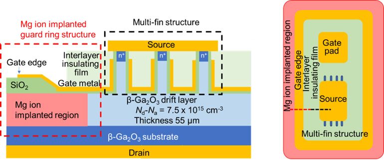
Figure 1. Schematic view of β-Ga2O3 MOSFET: (a) cross-sectional structure and (b) plan view.
Figure 1 shows the cross-sectional structure and plan view of the newly developed β-Ga2O3 MOSFET. Its features are as follows:
- a vertical device structure that is advantageous for low loss and high current required for power devices;
- a multi-fin structure with sub-micron mesa width channel that enables normally off operation without a p-type conductive layer;
- β-Ga2O3 drift layer with a low donor concentration of 7.5x1015cm-3, and a large thickness of 55μm;
- a guard-ring structure with Mg ion implantation into β-Ga2O3 in the area around the gate edge to reduce the electric field at the region.
The prototype β-Ga2O3 MOSFET has 10 fins with a mesa width of 0.2μm, a gate length of 3.5μm, a fin length of 70μm, and a fin pitch of 5μm.
Figure 2 shows the drain current–voltage characteristics of a prototype β-Ga2O3 MOSFET. It exhibits normally off characteristics in which no current flows at a gate voltage of 0V. The maximum current density normalized by the source electrode area (50μm x 60μm) is 218A/cm2, and the specific on-resistance is 21.6mΩ cm2 (Vgs=5V).
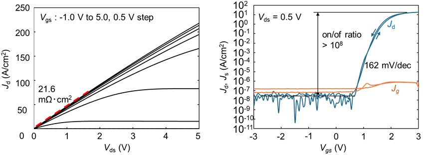
Figure 2. Drain current–voltage characteristics.
Figure 3. Drain current/gate current–gate voltage characteristics.
Figure 3 shows the dependence of the drain and gate currents on the gate voltage. The drain current on/off ratio is as large as eight orders of magnitude or more, and the subthreshold slope is 162mV/decade, resulting in good transistor characteristics.
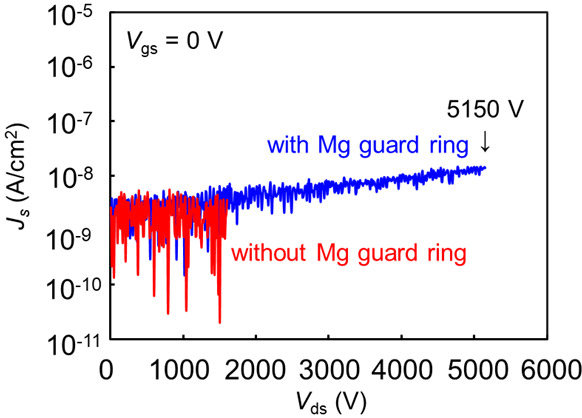
Figure 4. Transistor breakdown voltage waveform.
Figure 4 shows the source and gate current characteristics when the gate voltage and source voltage are fixed at 0V and a positive voltage is applied to the drain electrode. By applying a guard-ring structure with Mg ion implantation, the breakdown voltage was increased from 1.6kV to 5.15kV. The maximum electric field strength in the β-Ga2O3 drift layer before and after application of the guard-ring structure is estimated to be 2MV/cm and 3.72MV/cm, respectively. NCT believes that the Mg guard ring reduces the concentration of the electric field at the gate electrode end and makes it possible to increase the electric field strength in the drift layer.
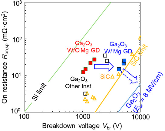
Figure 5. MOSFET characteristics: on-resistance and breakdown voltage.
Figure 5 shows the relationship between the specific on-resistance (Ron,sp) and breakdown voltage (Vbr), which is a performance indicator of power devices. The breakdown voltage was greatly improved by incorporating a guard-ring structure formed by ion implantation of Mg into β-Ga2O3 in the electrode termination region. As a result, it is 13.3 times greater than before the application of the guard ring, and a large PFOM value of 1.23GW/cm2 was obtained. This is a record for β-Ga2O3 FETs and is 3.2 times higher than the previous record.
Next steps
The termination structure of β-Ga2O3 MOSFETs is further enhanced by utilizing hetero p-type semiconductor materials such as NiO etc to further reduce the electric field concentration at the electrode termination. NCT aims to realize a β-Ga2O3 power transistor with performance exceeding that of SiC’s by exploiting the potential of β-Ga2O3’s high breakdown field strength (6–8MV/cm) with an advanced termination structure.
Mitsubishi Electric buys stake in Novel Crystal Technology
Novel Crystal Technology reports first inverted gallium oxide DI-MOS transistor


