


News: Microelectronics
12 August 2025
1200V fully vertical GaN-on-silicon MOSFETs
Shandong University and Huawei Technologies Co Ltd in China have used fluorine (F)-ion implantation termination (FIT) to achieve 1200V breakdown performance in fully vertical gallium nitride (GaN)-on-silicon (Si) trench metal-oxide-semiconductor field-effect transistors (MOSFETs) [Yuchuan Ma et al, IEEE Electron Device Letters, published online 8 July 2025].
Typically, mesa etching termination (MET) is used to electrically isolate GaN semiconductor devices. However, this results in relatively sharp corners where electric fields tend to crowd, causing premature breakdown. MET-MOS fully vertical MOSFETs have breakdown voltages around 650V.
Power GaN devices are competing with silicon carbide (SiC) transistors. While GaN has good performance in the 100–650V class, SiC tends to be commercially favored for 1200V applications. Achieving 1200V in devices on low-cost silicon substrates could tip the commercial balance towards GaN.
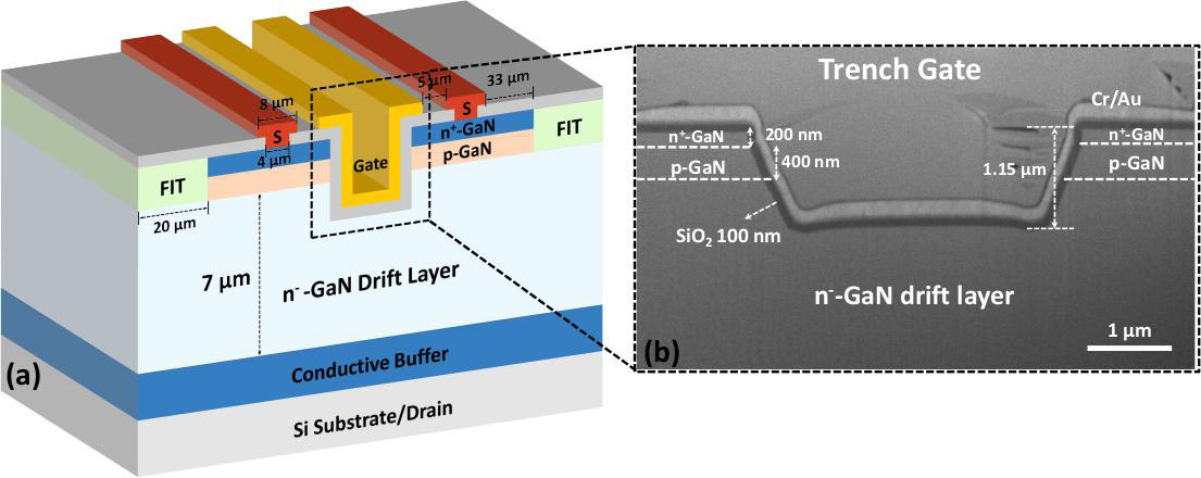
Figure 1: (a) Schematic structure and (b) cross-sectional scanning electron microscope (SEM) image (trench gate region) of fully vertical GaN-on-Si trench MOSFETs with fluorine implanted termination (FIT-MOS).
The fully vertical transistors (Figure 1) were fabricated using GaN/silicon metal-organic chemical vapor deposition (MOCVD) epitaxial material with a buried p-GaN layer.
The researchers comment: “The conductive buffer layer, composed of AlGaN/AlN multi-layers, enables a fully vertical current path while eliminating the need for a complex substrate engineering process to achieve the fully vertical configuration.”
The buffer also provided compressive stress, compensating for tensile stress in the overlying GaN layers that can build up during cooling after high-temperature MOCVD. Such tensile stress can lead to cracks without compensation. The researchers used x-ray analysis to estimate a threading dislocation density of 3.0x10⁸/cm2. The corresponding estimate from cathodoluminescence was 1.4x10⁸/cm2.
The gate trench was etched first. The p-GaN was activated by thermal annealing. The researchers also repaired the gate trench dry etch damage by tetra methyl ammonium hydroxide (TMAH) treatment.
The F-ion implantation was carried out at three energies (and doses): 240keV (4x10¹⁴), 140keV (2x10¹⁴) and 80keV (1.2×10¹⁴/cm2), respectively.
Atomic layer deposition (ALD) silicon dioxide (SiO2) was used as gate dielectric. The source contact windows were opened by reactive-ion etch. The source and gate metals were both chromium/gold. The drain contact consisted of the low-resistivity silicon substrate. The researchers also fabricated a device with a convention MET process for comparison purposes.
The FIT-MOS demonstrated enhancement-mode operation with a positive threshold voltage (VTH) of 3.3V. The on/off current ratio was of order 107. The on-state current density was 8kA/cm2. The specific on-resistance (Ron,sp) was 5.6mΩ-cm2, described as “relatively low”.
The breakdown voltage (BV) was 1277V, compared with 567V for the comparison MET-MOS (Figure 2). The team comments: “The FIT-MOS exhibits a larger OFF-state current density at low VDS than that of the MET-MOS due to the additional vertical leakage path associated with the FIT structure.”
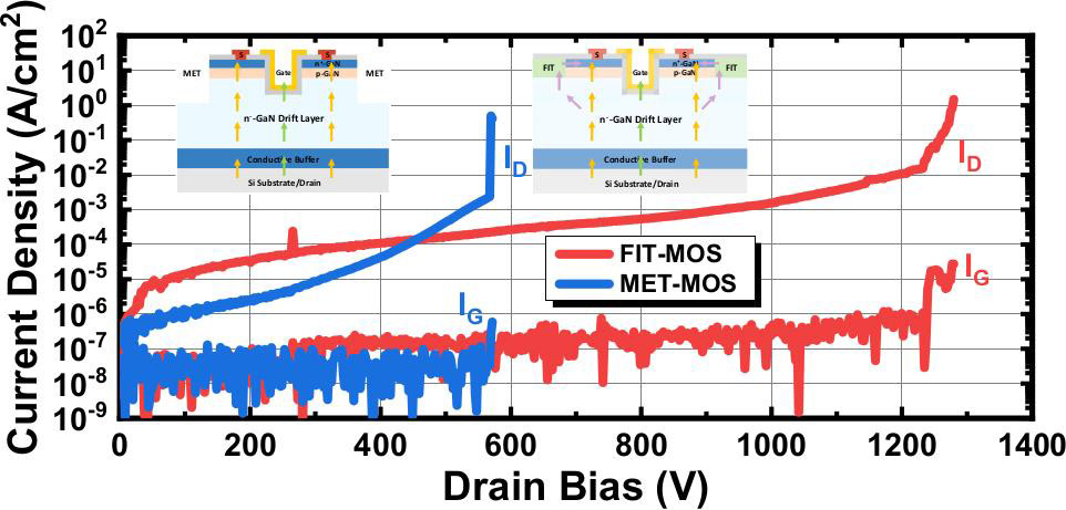
Figure 2: OFF-state breakdown current–voltage (I–V) characteristics at 0V gate potential (VGS) of fabricated fully vertical GaN-on-Si FIT- and MET-MOS. Inset: potential leakage paths of FIT- and MET-MOS.
The researchers also suggest that the F ions could diffuse through Ga vacancies and subsequently escape from the transistor material negatively impacting thermal stability. “Adopting an optimized post-implantation annealing process can efficiently reduce the OFF-state leakage current density as well as enhance the thermal reliability of the FIT-MOS,” the team writes.
Simulations by the researchers suggest that the FIT structure reduces electric field crowding, such as occurs at the corners of the mesa in MET-MOS transistors. The FIT simulation did show crowding near the gate trench. This could be ameliorated with gate shielding.
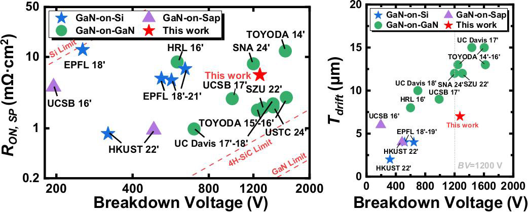
Figure 3: Benchmarks of (a) Ron,sp versus BV, and (b) drift-layer-thickness (Tdrift) versus BV, for fully vertical FIT-MOS against reported GaN vertical trench MOSFETs on silicon, sapphire (Sap), and GaN substrates.
The researchers also compare the Ron,sp, BV and drift layer thickness (Tdrift) performance of their FIT device against previously reported vertical GaN transistors (Figure 3). Combining the breakdown and on-resistance results in the BV2/Ron,sp Baliga figure of merit (BFOM) gave a value of 291MW/cm2, comparable to the value of devices fabricated on much more expensive native GaN substrates. At the same time, the FIT-MOS gave similar BV performance with a thinner drift layer, compared with such expensive GaN/GaN transistors (7μm, versus more than 10μm for 1200V BV).
GaN-on-silicon MOSFETs GaN MOSFETs Fluorine-ion implantation termination MOCVD
https://doi.org/10.1109/LED.2025.3586947
The author Mike Cooke is a freelance technology journalist who has worked in the semiconductor and advanced technology sectors since 1997.


