


News: LEDs
11 December 2025
Patterning GaN for improved red LEDs
Hefei University of Technology and Nanjing University in China have reported on the use of gallium nitride (GaN) template patterning as a means to enhance red light emission from high-indium-content quantum wells (QWs) in light-emitting diodes (LEDs) [Kun Xing et al, IEEE Transactions On Electron Devices, published online 18 November 2025].
The researchers found that the optimal template region was a 300μm x 300μm square on which the LED material was grown and then formed into devices.
The team reports: “A red mini-LED fabricated on the optimal template exhibited a peak emission wavelength of 634.0nm at 1A/cm2, with the peak EQE [external quantum efficiency] enhanced by 57% compared to the LED grown on the unpatterned template.”
Red mini-LEDs and micro-LEDs are being developed for micro-displays and other displays. At present the efficiencies are low, both for standard red-emitting semiconductors such as aluminium indium gallium phosphide (AlInGaP), and InGaN. AlInGaP in small form factors suffers from high surface recombination rates at sidewalls, killing efficiency. For InGaN, this has been found to be much less of a problem. Rather, it is still the high defect levels and other problems of incorporating sufficient indium to enable stable red light emission.
The researchers describe the effect of the template size on the GaN material grown on top: “The compressive stress within the lattice is relieved when the external lattice expands freely toward the periphery after the material surrounding the template has been etched away, inducing lateral relaxation of the internal lattice structure. Hence, the size of the patterned template is expected to influence the compressive strain within the GaN layer by affecting the degree of relaxation.”
The patterning was carried out in a GaN template layer on patterned sapphire substrates (PSS), using inductively coupled plasma (ICP) etch through a SiO2 mask (Figure 1). The pattern pitch was 20μm at an etch depth of 3μm. The patterning was performed in squares up to 500μm on a side.
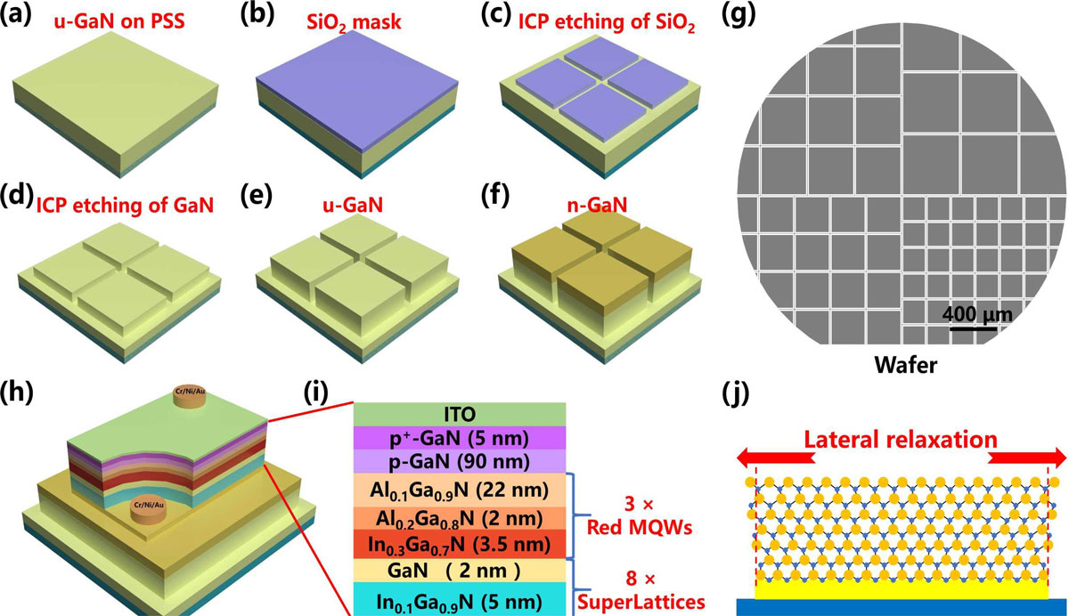
Figure 1: Template process scheme: (a) GaN on PSS; (b) deposition of silicon dioxide (SiO2) mask; (c) inductively coupled plasma (ICP) etching of mask; (d) ICP etching to expose GaN; (e) epitaxial undoped (u-)GaN layer; (f) epitaxial n-GaN layer. (g) Different dimensioned GaN templates fabricated on same epitaxial wafer. (h) Full structure of InGaN-based red mini-LED. (i) Red-emitting quantum well (QW) structure. (j) Atomic structure of laterally relaxed GaN layer.
The patterned template was used for metal-organic epitaxy of red LED structure with triple InGaN QWs with 30% indium content. Devices, 90μmx150μm, were fabricated with an indium tin oxide (ITO) current-spreading layer. The metal contacts were chromium/nickel/gold.
The tested LEDs were from the central region of the wafer to minimize wafer-edge growth issues. The LEDs themselves were fabricated near the center of each GaN tile, well away from etched boundaries. Also, reference devices (LED E) were fabricated on material on an unpatterned template processed in the same epitaxy furnace.
Reciprocal space mapping analysis of x-ray measurements showed that smaller template sizes encouraged lateral strain relaxation. Screw and edge dislocation densities were estimated from x-ray rocking curve behaviors. The screw dislocations were an order of magnitude lower than that for edge defects.
The lowest screw dislocation density of 1.63x10⁷/cm2 was found for the smallest template square region of side 200μm (LED D). The edge defects were lowest for the slightly larger 300μm squares of LED C: 3.06x10⁸/cm2. The researchers potentially attribute the increase in edge defects for the smallest patterned template region “to the emergence of sidewall defects during the etching process, which created pathways for the generation and propagation of edge dislocations.”
Table 1: Peak wavelength blue-shift and value at 10A/cm2 injection.
LED |
A | B | C | D | E |
| Template | 500μm | 400μm | 300μm | 200μm | N/A |
| Blue-shift 0.1–10A/cm2 | 45nm | 44nm | 40nm | 38nm | 60nm |
| Peak wavelength 10A/cm2 | 610.3nm | 610.4nm | 613.6nm | 618.8nm |
Electroluminescence (EL) studies showed reduced blue-shift of the spectrum with increased current injection (Table 1). The blue-shift was also lessened in the LEDs on reduced size templates. Such blue-shift effects are typically attributed to quantum-confined Stark effects (QCSEs) where lattice strain and charge polarization of the different materials lead to electric fields across the QWs that tend to discourage radiative recombination of electrons and holes, reducing light output, particularly in longer-wavelength devices.
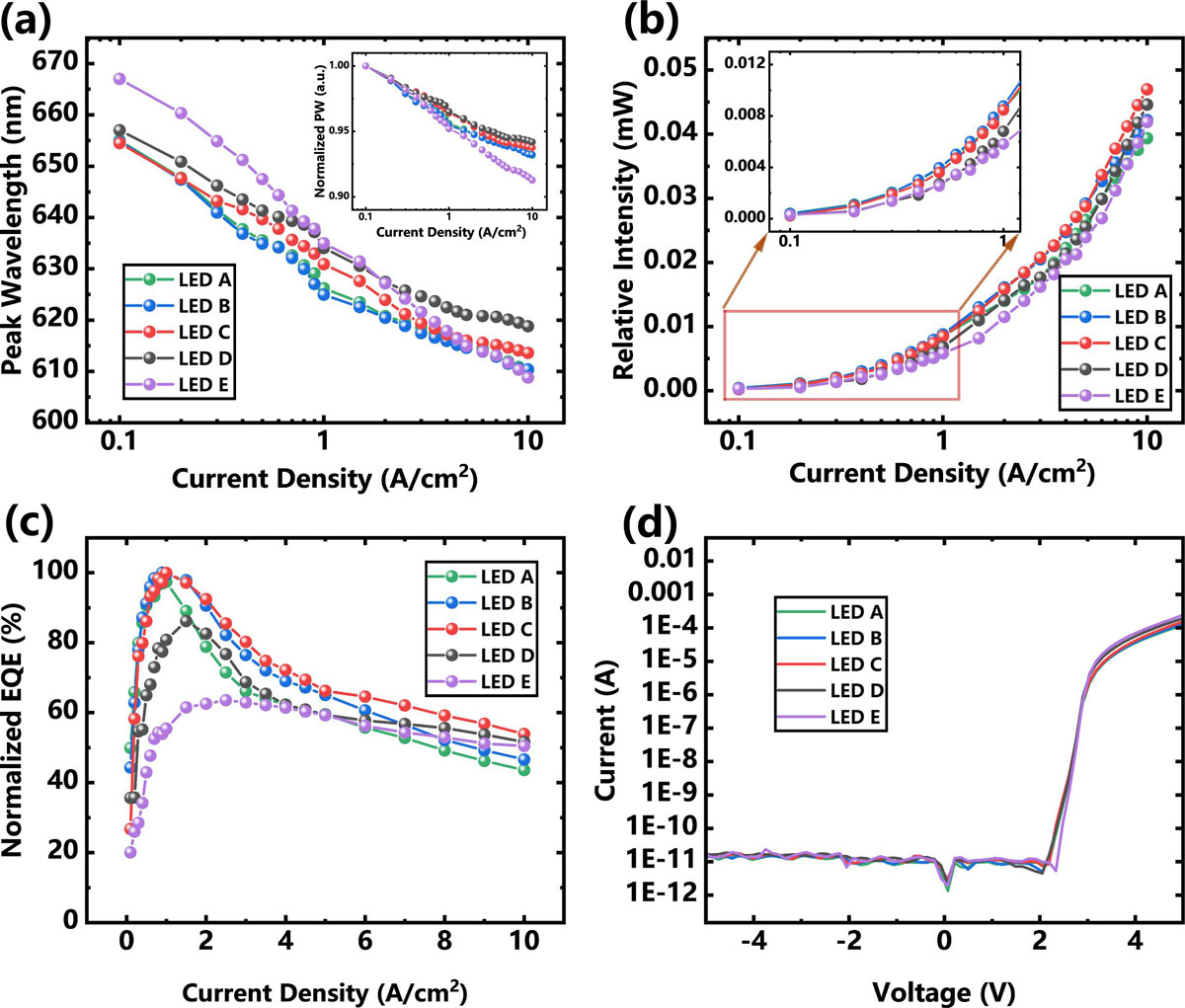
Figure 2: Current density dependences of prototype red InGaN-based mini-LEDs grown on GaN templates A–E. (a) Peak wavelength. (b) Relative luminous intensity. (c) Normalized EQE. (d) Current–voltage curves of LEDs A–E.
The researchers believe that the enhanced relaxation that comes with a reduced template size increased indium incorporation in the QWs, allowing LED D to maintain a longer peak wavelength at higher current injection (Figure 2).
In terms of emission intensity, LED C provides better performance. The researchers suggest that the degradation of LED D was the result of “degraded crystal quality, with a higher indium fraction typically leading to an increased defect density (e.g. V-defects or dislocations that form to relieve strain)”.
The external quantum efficiency (EQE) performance of LED C maintained an edge over the others. The reference LED E had a low EQE peak, but only slowly declined, almost matching the EQE of LED C at 10A/cm2.
The team comments: “We attribute LED E’s small droop to its higher density of dislocations and non-radiative recombination centers (due to the lack of strain-relief patterning) relative to the patterned LEDs, which leads to strong SRH recombination even at low and moderate currents. As a result, LED E’s EQE is already suppressed at low injection levels by defect-related SRH recombination. As the current density increases, SRH recombination becomes saturated at high currents, and the remaining efficiency droop is dominated by Auger recombination and leakage mechanisms, which are common to all LEDs.”
https://doi.org/10.1109/TED.2025.3630618
The author Mike Cooke is a freelance technology journalist who has worked in the semiconductor and advanced technology sectors since 1997.


