


News: Microelectronics
20 February 2025
AlScN-barrier GaN HEMT with record high on-current
Researchers in the USA claim record high on-current up to 4A/mm for gallium nitride (GaN) high-electron-mobility transistors (HEMTs) with an epitaxial aluminum scandium nitride (AlScN) barrier layer [Kazuki Nomoto et al, Appl. Phys. Express, v18, p016506, 2025].
The team, from Cornell University and Northrop Grumman Mission Systems Advanced Technology Laboratory, comments: “All AlScN-barrier GaN HEMTs show high output currents compared to conventional GaN HEMTs with AlGaN or InAl(Ga)N barriers with similar device designs. This is due to the larger polarization discontinuity of AlScN with GaN, thus a high channel charge.”
GaN devices are seeing deployment in areas needing high frequency, low noise, high linearity, high power, and reliable performance.
The Cornell team has been exploring AlScN as a high-k gate insulator due to its high thermal and chemical stability, and potential for lattice matching with GaN, with a view to enhanced intrinsic transconductance and breakdown voltage.
The researchers comment: “With expected future improvements in electron mobility and heterostructure design to enhance transconductance, these results demonstrate the great potential of AlScN to improve the output power and maximum speed of nitride-based millimeter-wave integrated circuits.”
The material for the HEMTs (Figure 1) was grown using plasma-assisted molecular beam epitaxy (PA-MBE) on 10mmx10mm silicon carbide (SiC) substrate.
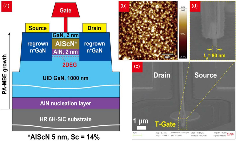
Figure 1: (a) GaN HEMT schematic cross-section. (b) Atomic force microscope (AFM) image of as-grown sample surface. (c) Scanning electron microscope (SEM) image of processed HEMT, and (d) zoomed-in on T-gate.
Hall-effect measurements before fabrication gave a sheet-resistance estimate of 417Ω/□, based on a two-dimensional electron gas (2DEG) sheet-carrier density of ~3x10¹³/cm2 and 419cm2/V-s mobility. After HEMT fabrication the mobility was maintained, but the carrier density reduced to ~2.2x10¹³/cm2. The researchers point to previous work at Cornell showing that mobility in AlScN/GaN structures can reach 1500cm2/V-s.
The team comments: “The mobility of our sample is reasonable considering the unoptimized GaN buffer growth on 6H-SiC, thus the interface roughness near where the 2DEG resides in this study. The lower mobility compared to prior works can also be attributed to the higher sheet charge density observed in our samples arising from a higher Sc composition. This higher charge density contributes to an enhanced device output current, even though it increases scattering effects, which slightly reduces mobility. The tunability of AlScN properties in terms of strain balance and ferroelectricity affords a wide range of potential applications.”
The material was patterned with a silicon dioxide/chromium mask and etched to a depth of 40nm before PA-MBE regrowth of 100nm n+-GaN for the source and drain contact structures. The high-k AlScN layer in the barrier layer was 5nm thick. The metal for the source/drain contacts was non-alloyed titanium/gold, and the T-gate consisted of nickel/gold.
A 2x25μm-wide device with 90nm gate and 600nm source–drain distance demonstrated a maximum drain current of 4.07A/mm and 0.59Ω-mm on-resistance at 0V gate potential (Figure 2). The peak transconductance at 5V drain bias was 0.50S/mm.
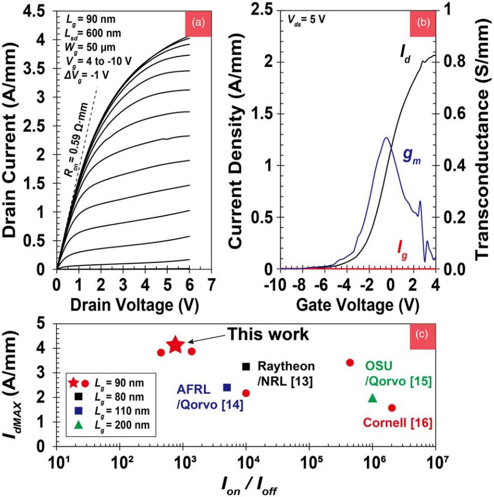
Figure 2: (a) Drain current–voltage output characteristics from gate potential sweep, and (b) transfer characteristics. (c) Output current benchmark of AlScN HEMTs with previous reports.
The researchers comment on the lower maximum drain current (2.1A/mm) for the transfer measurements performed after the output measurements (4.07A/mm): “This decrease in current density for scaled devices and ultra-thin barrier layers after several measurement cycles is not unexpected since the devices were not passivated.”
The frequency performance of the device was measured between 50MHz and 50GHz, resulting in 92.4/134.3GHz de-embedded current gain cutoff (fT)/maximum oscillation (fMAX) frequencies. The best RF performance from fT/fMAX mapping was achieved at 6V drain bias with 3.13A/mm on-current.
The team also studied three-terminal off-state breakdown behavior in devices with gate-drain distances varying between 0.25μm and 3.85μm (Figure 3). There was a spread of breakdown voltages (BV) for devices with the same gate–drain distance. The team suggests this was due to non-uniformity of the channel electric field profile within the different devices. The maximum BV was 78V in a device with 3.85μm, giving a laterally averaged electric field of 0.2MV/cm. Devices with shorter gate–drain drift regions had higher breakdown electric field averages, but with lower BV overall.
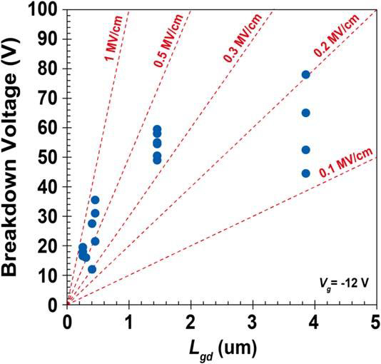
Figure 3: Breakdown voltage as function of gate–drain separation.
The team comments: “During the measurement and prior to breakdown, the gate current is found to be roughly equal to the drain current. This indicates that the off-state drain current and breakdown is dominated by gate–drain leakage, not avalanche or channel breakdown, and is far from intrinsic material limits. The breakdown mechanism appears to be a hard breakdown.”
Optical inspection showed structural damage around the gate and drain electrode edges. The researchers point out that “these regions are subject to the highest electric field intensities during device operation.”
The team also admits that the BV values were lower than expected, given the high-k nature of the AlScN. “Typically, AlN-GaN RF HEMTs show breakdown electric fields upwards of 1–2MV/cm. This points to room for improvement in the insulating behavior of the AlScN layer.”
With 455nm gate–drain, the BV was 35.5V, demonstrating an average electric field of 0.78V/cm. The best BV×fT Johnson figure of merit (JFOM) for the HEMT devices was ~1.8THz-V.
The team believes that the BV can be increased with the use of passivation and field plates designed to make the electric field more uniform in the drift region, reducing the peak electric field and thus delaying breakdown.
Apart from the Northrop Grumman Mission Systems financial contribution, the research also received support from the Semiconductor Research Corporation (SRC) and the Joint University Microelectronics Program 2.0 (JUMP 2.0), organized by the US Defense Advanced Research Projects Agency (DARPA).
GaN HEMTs GaN HEMTs AlScN barrier layer
doi.org/10.35848/1882-0786/ada86b
www.darpa.mil/research/programs/jump
The author Mike Cooke is a freelance technology journalist who has worked in the semiconductor and advanced technology sectors since 1997.


