


News: Microelectronics
18 February 2025
Infineon launches CoolGaN G3 Transistor in new silicon-footprint packages
Since gallium nitride (GaN) suppliers have taken various approaches to package types and sizes, leading to fragmentation and a lack of multiple footprint-compatible sources for customers, Infineon Technologies AG of Munich, Germany has launched the high-performance CoolGaN G3 Transistor 100V in RQFN 5x6 package (IGD015S10S1) and 80V in RQFN 3.3x3.3 package (IGE033S08S1).
“The new devices are compatible with industry-standard silicon MOSFET packages, meeting customer demands for a standardized footprint, easier handling and faster-time-to-market,” says Dr Antoine Jalabert, product line head for mid-voltage GaN at Infineon.
The CoolGaN G3 100 V Transistor devices will be available in a 5x6 RQFN package with a typical on-resistance of 1.1mΩ. Additionally, the 80V transistor in a 3.3x3.3 RQFN package has a typical resistance of 2.3mΩ.
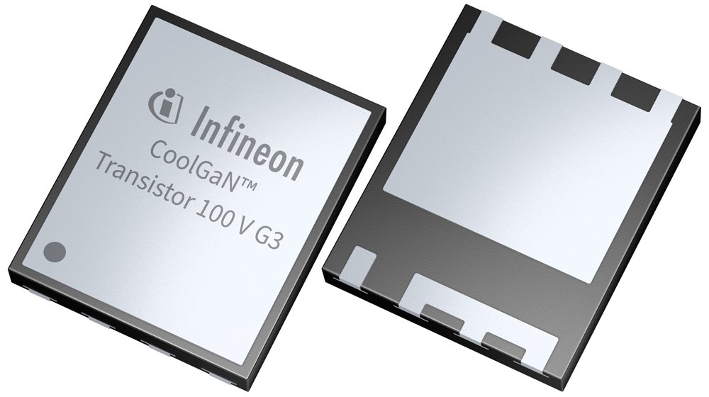
Picture: CoolGaN G3 Transistor in new silicon-footprint packages.
The transistors offer a footprint that, for the first time it is claimed, allows for easy multi-sourcing strategies and complementary layouts to silicon-based designs. In combination with GaN, the new packages offer a low-resistance connection and low parasitics, enabling high-performance transistor output in a familiar footprint.
Moreover, the chip and package combination allows a high level of robustness in terms of thermal cycling, in addition to improved thermal conductivity, since heat is better distributed and dissipated due to the larger exposed surface area and higher copper density.
Samples of the GaN transistors IGE033S08S1 and IGD015S10S1 in RQFN packages will be available in April.
Infineon launches CoolGaN transistor families built on 8-inch foundry processes


