


News: Optoelectronics
6 February 2025
InGaN laser diodes on c-plane lateral overgrowth material
University of California Santa Barbara (UCSB) in the USA reports successful demonstration of indium gallium nitride (InGaN) edge-emitting laser diodes (EELDs) on fully coalesced epitaxial lateral overgrown (ELO) films from a c-plane GaN substrate [HSun-Ming Chang et al, Jpn. J. Appl. Phys., v64 p010903, 2025].
The team reports: “By optimizing the crystalline quality, particularly in the wing regions, a significant reduction in threading dislocations is achieved, leading to a 21.4% to 25.6% reduction in threshold current density and up to 50% improvement in slope efficiency.”
Such EELDs have seen deployment in automotive lighting, material processing, and solid-state lighting. Emerging applications include portable, battery-powered augmented/virtual-reality (AR/VR) displays, and projectors. Wider commercial use would hinge on factors such as improved differential efficiency, lower current thresholds, and longer operational life, at low cost. The cost factor is hampered by the need to use native GaN substrates, and further by the need in many applications to use non-polar or semi-polar GaN substrates, which are only available in smaller sizes than polar c-plane (0001) material.
The UCSB has previously developed its ELO processes on these small, expensive non- or semi-polar GaN substrates. In particular, the group has focused on expanding the high-crystal-quality regions.
The researchers comment: “While traditional ELO techniques have been limited by small wing regions, our specialized approach offers wider, high-quality epitaxial layers suitable for advanced optical devices like EELDs and VCSELs.”
They add: “By demonstrating a direct correlation between threshold current reduction and epitaxial layer quality, we aim to show that ELO advancements can be effectively applied to more accessible and cost-efficient c-plane GaN EELDs.”
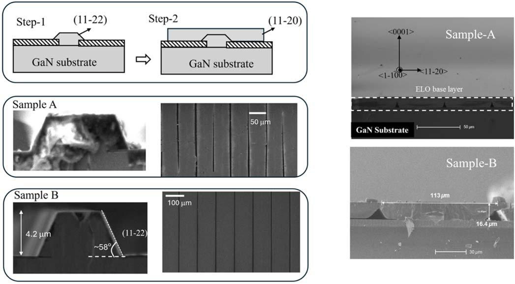
Figure 1: (a) Two-step growth process scheme; (b) Cross-sectional scanning electron microscope (SEM) images of Samples A and B with 55μm and 110μm periodicity, respectively; (c) fully coalesced ELO base layers.
The researchers used native c-plane (0001) GaN substrates with a threading dislocation density (TDD) better than 5x10⁶/cm2, supplied by Sumitomo Chemical. The ELO growth mask consisted of a 1μm silicon dioxide (SiO2) layer with 5μm windows parallel to the m-axis of the crystal structure (Figure 1). The patterning used conventional photolithography techniques.
Two samples, A and B, were distinguished by separations between the window stripes of 55μm and 110μm for samples A and B, respectively. Sample A was the main focus of the research, while sample B was designed to explore the feasibility of scaling the ELO layers to have wider wings for fabricating higher-power laser diodes.
The pattern was wet etched into the SiO2, exposing the GaN and undercutting the SiO2 sidewalls. The windows unintentionally expanded from 5μm to 8μm in width.
The ELO process consisted of two metal-organic chemical vapor deposition (MOCVD) steps. In the first step, a GaN post is developed with an 1080°C/760Torr MOCVD recipe with the ammonia (NH3) nitrogen precursor alternated in 5-second pulses, while the trimethyl-gallium (TMG) precursor flow was 13 standard cubic centimeters/minute (sccm). The ammonia flows in the two pulse durations were 0.8 and 13.7 standard liters/minute (SLM). The flow of hydrogen carrier gas was suitably modified to maintain the pressure in the chamber.
The researchers explain: “This creates an environment with a low V/III ratio, which is conducive to the growth of the (11−22) and (11−20) crystal planes. These planes are crucial for forming GaN-posts within the open windows between the SiO2 mask layers.”
Once the GaN posts were formed, the MOCVD process changed to one designed to laterally expand the GaN layer over the SiO2 dielectric mask with alternate NH3 gas flows of 0.2SLM for 5 seconds and 0.1SLM for 10 seconds. As the wings extended, the NH3 was gradually increased to 3.2SLM.
The team comments: “This controlled growth mitigates stress at the coalescence interfaces with the neighboring GaN-post sidewalls, leading to the formation of a flat, fully coalesced ELO base layer.”
Using this technique, large wing width-to-height aspect ratios up to 5.9 were achieved on sample B.
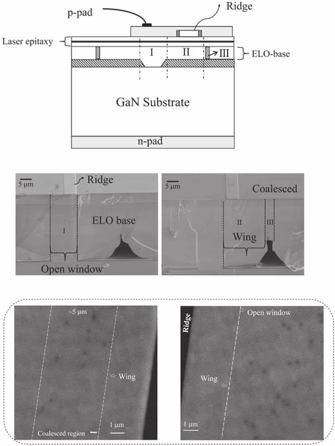
Figure 2: (a) EELD scheme fabricated on region-II of fully coalesced ELO base; (b) and (c) SEM cross-sectional images for two designs, with ridge positioned on open window and wing regions, respectively; (d) cathodoluminescence (CL) image of epitaxial layers formed on ELO base, covering all three regions.
The ELO material was used as a base for laser diode structures grown by MOCVD (Figure 2). The first layer, an n-GaN buffer, was grown at more than 1100°C. Subsequent layers were: 110nm n-InGaN buffer, 5-period 16/4nm InGaN/GaN superlattice, 60nm n-InGaN waveguide, multiple quantum well (MQW) active region, 10nm p-AlGaN electron-blocking layer, 60nm p-InGaN waveguide, 210nm cladding, and 15nm heavily doped p-GaN contact. The MQW sequence consisted of 2.5nm InGaN well, 2nm AlGaN cap, and 9nm GaN barrier (grown at +60°C higher than the well/cap layers).
The laser diode was fabricated with a shallow ridge dry etched and insulated with SiO2. The insulation was removed from the top of the ridge, and indium tin oxide (ITO) transparent conductor applied, providing a p-contact and extending the optical cladding. The p-metal contact pads were titanium/gold. The laser facets were formed with chemically assisted ion-beam etching (CAIBE). According to the team, this provides precise control over the facet quality, and minimizes surface damage. The bottom n-pad was titanium/aluminium/nickel/gold.
Two varieties of laser diode were fabricated: one with the ridge over the window region (I) of the of ELO base, and the other over the wing region (II). The coalescence region between neighboring ELO stripes was labeled as “region III”.
CL inspection of the laser diode structures showed the TDD to be less than 5x10⁵/cm2 in the wing region II, but this increased to 3.6x10⁷/cm2 over the window region and 2.6x10⁷/cm2 in the coalesced region.
The researchers comment: “These TDD values align with previous studies and demonstrate the superior crystalline quality in the wing region.” They add: “By avoiding the ~8μm open window and ~5μm coalescence region, we demonstrate a high usable low-TDD area for devices, which is approximately 76% in a 55μm-period sample (Sample A) and 88% for a 110μm-period sample (Sample B). The numbers in this work are amongst the best reported values in the literature.”
The team also suggests that its ELO technique could be extended to growth on GaN template layers on substrates such as sapphire, etc.
The ELO laser diodes fabricated in the wing region reached 0.17W/A single-facet slope efficiency with 3.63kA/cm2 threshold. The ridge was 7.5μm wide, and the cavity 1800μm long. The emission was around 408nm wavelength with 0.28nm full-width at half-maximum (close to the resolution limit of the spectrometer).
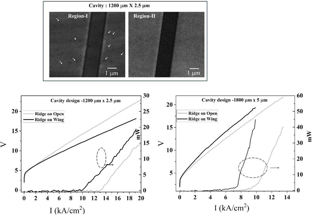
Figure 3: (a) CL images for 1200μmx2.5μm-cavity design for two types of laser, white arrows indicate TDs; (b) and (c) light output power−current−voltage (L−I−V) characteristics of two cavity designs on window/wing regions.
The laser diodes fabricated on wing regions outperformed the one on the window openings (Figure 3) in terms of lower threshold (−25.6%) and higher slope efficiency (+50%). The impact on operating voltages was less clear in terms of performance, where lower voltage indicates better power efficiency. The researchers comment: “The higher operating voltage observed in these devices is likely due to non-optimized p-doping in the cladding and waveguide structures.”
InGaN laser diodes InGaN GaN Substrates ELO MOCVD
https://doi.org/10.35848/1347-4065/ad9e5d
https://www.sumitomo-chem.co.jp/english/
The author Mike Cooke is a freelance technology journalist who has worked in the semiconductor and advanced technology sectors since 1997.


