


News: Optoelectronics
27 February 2025
Crack-free low threading dislocation density AlGaN for sub-365nm UV
University of Science and Technology of China, and Suzhou Institute of Nano-Tech and Nano-Bionics, claim the lowest 6.65x10⁸/cm2 threading dislocation density (TDD) for crack-free aluminium gallium nitride (Al0.2Ga0.8N) grown on unpatterned sapphire [Y. Q. Li et al, J. Appl. Phys., v137, p065703, 2025].
The researchers hope that producing higher-quality Al0.2Ga0.8N will lead in turn to high-performance AlGaN-based UVA optoelectronic devices, and in particular laser diodes (LDs) for the near-ultraviolet (UVA, 315–400nm) wavelengths below 365nm. Near-UV radiation also plays a role in industrial curing processes, along with 3D printing, biological sensing, etc.
The team reports on the difficulties sub-365nm: “In the spectral range above 365nm, low-threshold-density GaN-based laser diodes operating in continuous-wave mode with a long lifetime are already commercially available. AlGaN-based UVA laser diodes with wavelength below 365nm have not achieved room-temperature continuous-wave operation. One of the major challenges that UVA laser diode at emission wavelength below 365nm has faced is no such suitable substrate to grow the thick AlGaN cladding layer with aluminium composition around 20%.”
The researchers performed two-step growth (TSG) by metal-organic chemical vapor deposition on sapphire substrates with 25nm sputtered AlN films as nucleation. The Ga and Al metals were supplied as trimethyl (TMG/TMA) organic precursors; the N species came from ammonia (NH3).
Table 1: Growth conditions for samples with description of step I character.
Sample |
AlN thickness | Growth rate I/II | V/III ratio I/II | Description |
| A | 0μm | 0.36nm/s | 800 | Direct |
| B1 | 1μm | 0.37/0.37nm/s | 800/800 | Fast rate reference |
| B2 | 1μm | 0.18/0.37nm/s | 800/800 | Low rate |
| B3 | 1μm | 0.18/0.37nm/s | 2000/800 | High V/III |
| B4 | 1μm | 0.17/0.37nm/s | 500/800 | Low V/III |
Five Al0.2Ga0.8N samples were grown under different process conditions (Table a). Sample A was grown directly on the sputtered substrates with a single-step MOCVD. The samples Bn included a 1μm regrown AlN layer, a varied initial AlGaN growth step (I), and a final step II, which was the same for all Bn. B1 was grown under the same conditions as A, except for the regrown AlN layer, making it a reference for samples B2–4.
The regrown AlN was processed at 1300°C/100mbar with a V/III ratio of 350. The AlGaN growth was at 1200°C/200mbar. The growth rate and V/III ratios were controlled via the precursor flow rates into the hydrogen carrier gas.
The growth process was monitored using in-situ reflectance measurements. The reflectance oscillated over time through Fabry–Pérot interference as the layers became thicker.
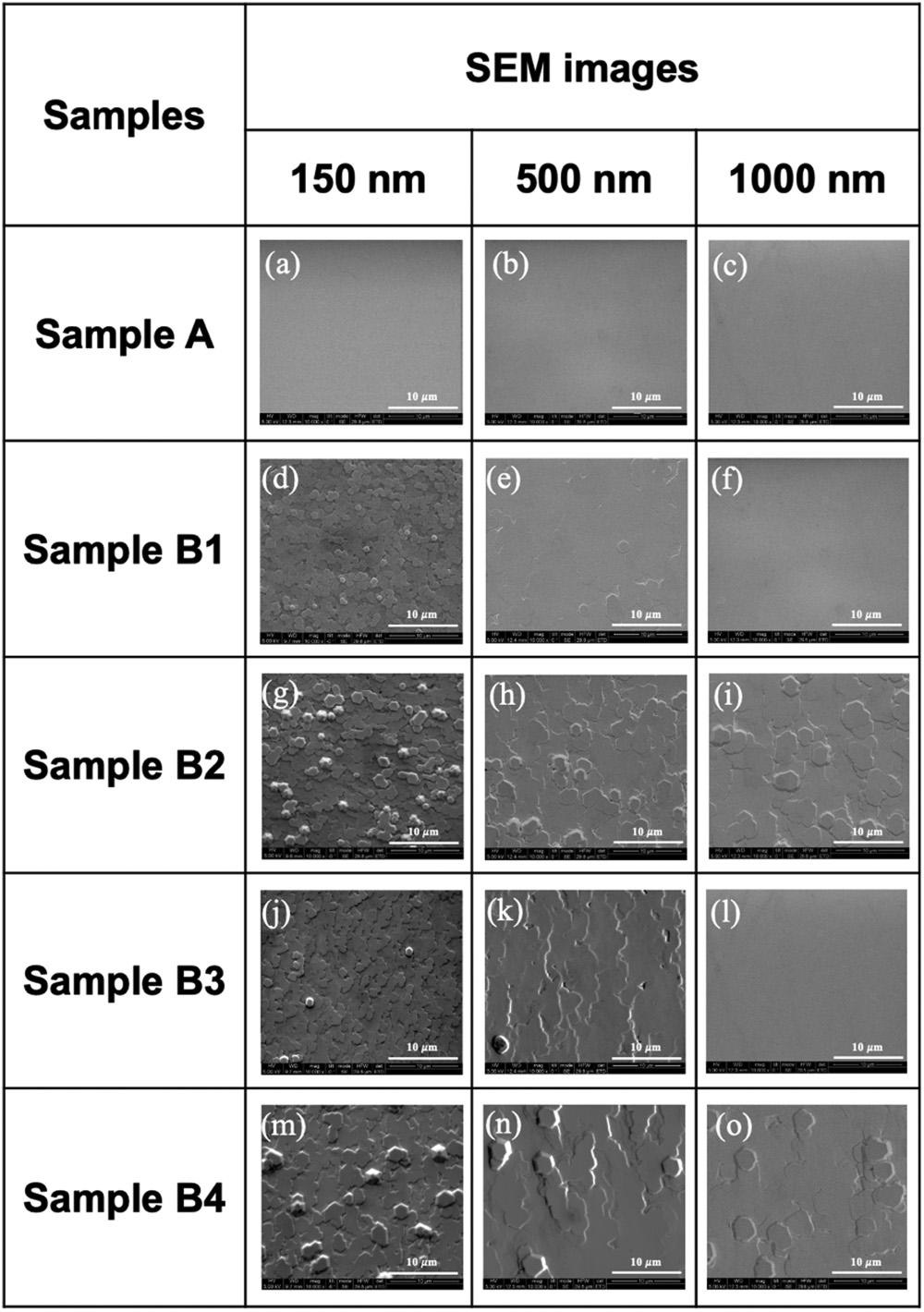
Figure 1: SEM images of the 3D stage of samples obtained by (a)–(c) direct 2D growth (DTG); (d)–(o) TSG with different growth rates and V/III ratio.
The two-step process proceeded initially with Stranski–Krastanov (SK) ‘layer-plus-island’ growth, followed by two-dimensional (2D) ‘layer-by-layer’/3D growth, according to the reflectance measurements and scanning electron microscopy (SEM) surface inspection of samples for which the growth was interrupted (Figure 1). By contrast, sample A showed just direct 2D growth.
The island growth enables strain relaxation, where the strain arises from the lattice mismatch between AlN and Al0.2Ga0.8N. In particular, the reflectance intensity decreased during step I, before picking up as the 3D growth transformed and coalesced into the 2D mode. The biaxial strain relaxation in B4 was estimated at 85%, according to high-resolution x-ray diffraction (HRXRD) reciprocal space mapping (RSM).
HRXRD was also used to assess the threading dislocation densities of the various samples. The lowest TDD estimate was for B4 at 6.65x10⁸/cm2, compared with 1.2x10¹⁰/cm2 for A. This was based on the full-width at half maximum for the [10-12] plane rocking curves reducing from 1032arcsec for sample A to 260arcsec for B4. The [0002] curves were by contrast almost the same: 160arcsec for sample A, and 159arcsec for B4.
The researchers comment: “It is known that the FWHM values of [0002] and [10-12] are proportional to the screw and edge dislocation densities in the samples, respectively. So, these results indicate that the 3D growth stage contributes to reduce edge dislocation density. Previous research studies have shown that edge dislocation is more bendable than the screw dislocation, which is consistent with our results.”
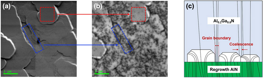
Figure 2: (a) SEM and (b) panchromatic CL images of coalescence stage; (c) schematic diagram of dislocation bending annihilation.
The researchers compared SEM and cathodoluminescence (CL) images to study TDD locations (Figure 2): dislocations were found to concentrate in the coalescence regions, while the middle of the larger islands were almost dislocation free. The team reports that “the larger island size and the lower island density resulted in fewer crystalline defects when the islands coalesce.”
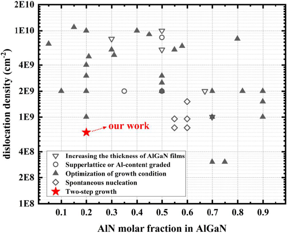
Figure 3: Relation between AlN molar fraction and dislocation density of AlGaN with more than 1μm film thickness.
Comparing with other works, the researchers claim the lowest dislocation density for AlGaN samples with the same composition and using unpatterned sapphire substrate (Figure 3).
https://doi.org/10.1063/5.0249836
The author Mike Cooke is a freelance technology journalist who has worked in the semiconductor and advanced technology sectors since 1997.


