


News: Microelectronics
13 February 2025
Gallium oxide JFETs reach beyond 10kV breakdown
Researchers based in USA and Japan report the demonstration of more than 10kV enhancement-mode (E-mode) gallium oxide (Ga2O3) lateral junction field-effect transistors (JFETs) with nickel oxide (NiO) reduced-surface-field (RESURF) structures and hybrid-drain, operating up to 250°C [Yuan Qin et al, IEDM, session 25-5, 2024].
The team from Virginia Tech and the US Naval Research Laboratory in the USA and Novel Crystal Technology in Japan presented their work at the IEEE International Electron Devices Meeting (IEDM 2024) in December. The researchers comment: “Our device demonstrates the highest average E-field, as well as the first report of 250°C operation and 3kV reliability data in a high-voltage transistor beyond silicon carbide (SiC).”
Ga2O3 has an ultra-wide bandgap (UWBG) of 4.8eV, compared with 3.4eV for gallium nitride (GaN) and up to 3.3eV for SiC. The 10kV breakdown performance puts the JFETs in the mid-voltage (1–35kV) range of power electronics devices with potential for wide deployment in power supply grids and renewable energy installations.
The researchers comment: “The availability of high-voltage (HV) devices can significantly reduce the device count, simplify the circuit topology, and improve the system form factor and reliability. Today’s commercial HV devices are dominated by silicon IGBTs up to 6.5kV; SiC MOSFETs are available in engineering samples up to 10kV”
Further, unlike other WBG materials, Ga2O3 is available in substrate wafers up to 6-inch in diameter. The crystal material can be grown from melt. Enhancement-mode (normally-off, i.e. current blocking at zero gate potential) transistors are generally preferred for power electronics, giving lower power consumption and fail-safe operation.
The device design (Figure 1) mainly sought to maximize performance in terms of E-mode operation, charge balance, and on-resistance (RON) operation. The device incorporated an n-type Ga2O3 channel, hybrid p-NiO/metal drain, heavily p-doped nickel oxide (NiO) gate, and p-NiO reduce-surface-field (RESURF) structure.
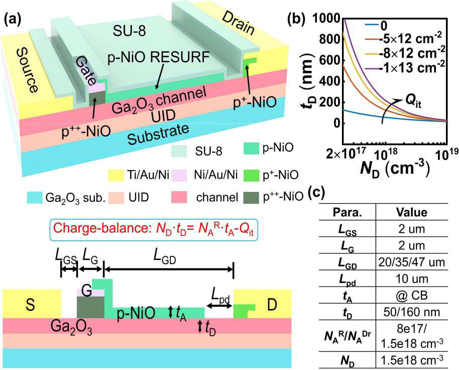
Figure 1: (a) Schematics of Ga2O3 JFET with p-NiO RESURF and hybrid drain designs: three-dimensional (top) and cross-section (bottom). (b) Calculated max channel thickness (tD) versus donor doping concentration (ND) to achieve E-mode, for interface charge (Qit) density from 013/cm2 to −1013/cm2. (c) Table of key device parameters and values.
The NiO regions were separated between the gate RESURF (R) and hybrid drain (Dr) sides to avoid punch-through. Also, the p-type doping concentrations on each side of the gap could be optimized separately (NAR/NADr). The RESURF structure design was similar to that of Infineon’s commercial gallium nitride GaN gate injection transistors (GITs).
The epitaxial material was grown on semi-insulating (010) Ga2O3 substrate by molecular beam epitaxy (MBE) with the n-type channel grown on an unintentionally doped (UID) layer. Two samples were produced, #A and #B, differing in the donor n-channel layer thickness (td) of 50nm and 160nm, respectively. A thicker channel should enable lower RON.
The device fabrication started with silicon implantation and activation, and deposition of the source/drain metals. The devices were electrically isolated by nitrogen-ion implantation.
The NiO materials were deposited using sputtering with the oxygen partial pressure being altered to create different acceptor levels in the sequence: hybrid drain, p++-gate, and RESURF regions. The gate doping level was more than 1019/cm3.
The threshold voltage (VTH) of #A and #B reached up to 1.9V and 1.5V, respectively, enabling E-mode operation. The gate potential was limited by gate leakage to around 3.5–4V. The corresponding specific on-resistances (RON,SP) were 703mΩ-cm2 and 92mΩ-cm2.
The researchers comment: “The 7x higher RON in device #A, despite a 3.2x thinner tD, implies a significant contribution of RON from the gated channel, where the non-depleted Ga2O3 channel for current conduction under the gate is much narrower in device #A.”
Increasing the device temperature to 250°C, reduced the VTH of the #A device to 0.7V, and increased the RON 1.6x, over the result at 25°C.
The team writes: “The T-coefficient of RON is smaller than that reported in a 10kV SiC MOSFET, suggesting a lower conduction loss at high T.”
The VTH of the #B JFET turned negative around 100°C, dropping to −3.3V at 150°C. Beyond 175°C, there was insufficient gate control of the device for it to be useful as a transistor.
With the gate potential at 0V, the breakdown voltage (BV) of devices on both samples exceeded 10kV. Maximal BV was enabled by adjusting the device parameters to a near charge balance condition. The highest BVs were enabled by the largest gate-drain spacing (LGD) of 47μm.
The team reports: “The average lateral E-field at BV is 1.75~2.45MV/cm.”
The #A devices maintained high BV at elevated temperatures up to 250°C. The #B material suffered at higher temperature, with the BV falling below 10kV at 150°C at −10V gate potential.
The researchers also performed high-temperature gate-bias/reverse-bias (HTGB/HTRB) reliability tests at 150°C.
For the HTGB test the threshold and on-resistance shifts varied within 0.32V and 35%, respectively, for both #A and #B devices in a fully recoverable manner.
The HTRB study of #B devices apparently showed drain-induced barrier lowering (DIBL) effects with a mostly recoverable VTH shift of −3V.
The researchers explain: “The thick channel in device #B leads to a lower barrier and punch-through at high VD. This DIBL can be deteriorated by the Qit and its accelerated de-trapping at high T.”
The threshold shift for #A devices was within 0.2V, while the on-resistance increased by 34%. The parametric shifts for #A were fully recoverable, according to the researchers. Of course, the drawback for devices on sample #A was a higher on-resistance due to the narrower channel.
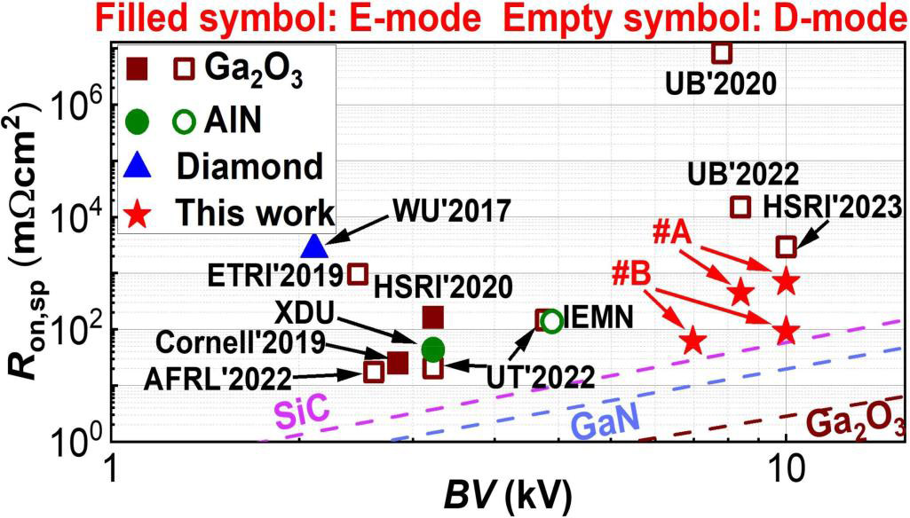
Figure 2: RON,SP versus BV benchmark against state-of-the-art UWBG power transistors with BV >2kV. Colored dashed lines show various theoretical limits for different semiconductor materials (SiC/GaN/Ga2O3).
Comparing the RON,SP and BV performances with the literature (Figure 2), the researchers report figures of merit (FOMs, BV2/RON,SP) of at least (BV>10kV) 142MW/cm2 and 1086MW/cm2 for devices #A and #B, respectively. These values are claimed as “a new record in all UWBG transistors with BV >3kV.” The team adds: “Device #A is also the first E-mode device reported in all >3kV UWBG transistors.”
https://iedm24.mapyourshow.com/
The author Mike Cooke is a freelance technology journalist who has worked in the semiconductor and advanced technology sectors since 1997.


