News: Optoelectronics
23 January 2025
Gallium arsenide nano-ridge laser diodes on 300mm silicon
Researchers working in Belgium claim record-low crystal defectivity in epitaxially grown gallium arsenide (GaAs) on silicon (Si) used as the base for nano-ridge (NR) quantum well laser diodes (LDs) fabricated on a 300mm CMOS pilot line [Yannick De Koninck et al, Nature, v637, p63, 2025]. It is hoped that the work will lead on to low-cost integration of III–V light sources with silicon photonics and electronics, compared with heterogeneous integration techniques such as wafer–wafer or chip–wafer bonding.
The researchers at IMEC, Katholieke Universiteit (KU) Leuven, and Ghent University–IMEC, claim a 6x10⁴/cm2 misfit defect density, which compares very favorably with other heteroepitaxy reported densities in the (1.5–26)x106/cm2 range. The NRs were produced in 1μm-pitch arrays.
The team used aspect-ratio trapping (ART) to reduce the formation of threading dislocations (TDs) in the NR structures (Figure 1). The trapping ensures that most TDs terminate on the trench walls, rather than escaping into the body of the device, impacting performance.

Figure 1: a, Fabricated 300mm silicon wafer with thousands of GaAs devices. b, Close-up view showing several dies. c, Cross-sectional scanning electron micrograph (SEM) after epitaxy and before oxide encapsulation.
The NR structure also reduces major issues such as the wafer bow and crack formation typical in blanket III–V epitaxy on silicon.
The 300mm silicon wafers were n-type doped. The NRs were initiated with growth of n-GaAs in high-aspect-ratio trenches in the n+-Si wafer using metal-organic vapor phase epitaxy. The bottoms of the trenches were V-shaped with {111} facets, which are advantageous for high-quality GaAs growth.

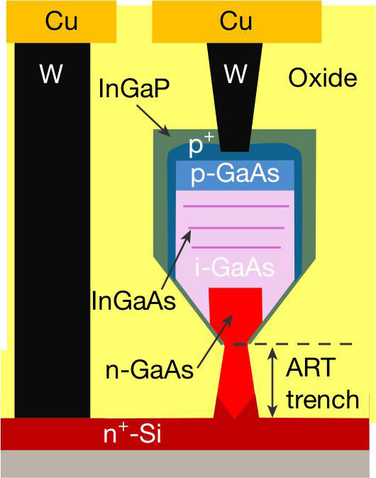
Figure 2: Cross-sectional sketch of GaAs NR device.
The further laser diode layers were also grown by MOVPE on the n-GaAs stub (Figure 2). The active region consisted of three indium gallium arsenide (InGaAs) quantum wells containing 20% indium separated by undoped GaAs (i-GaAs) barriers. The wells were compressively strained. The device growth was completed with p-GaAs contact layers and indium gallium phosphide (InGaP) passivation.
The diodes had a p-i-n structure. Standard copper (Cu) metalization processes were used to fabricate the external connections to the laser structures via tungsten (W) plugs. These metalization processes are widely used in mainstream complementary metal-oxide-semiconductor (CMOS) electronics manufacturing.
Some laser cavities were formed with facets at a 12° angle to give 5% reflectivity. The laser output was monitored on one side with on-chip photodetectors formed from the same material. The other facet fed into an etched region of the wafer designed to allow out-of-plane optical emission.
The researchers varied the pitch between the W plugs connecting to the p-side of the diode along the laser cavity. With a 4.8μm pitch the NR laser diode achieved efficient lasing. The researchers comment: “In these designs, mode beating of the fundamental TE00 and the higher-order TE01 mode results in a periodic interference pattern that minimizes the optical intensity locally underneath the W plugs.”
By contrast, a 3.0μm W-plug pitch resulted in strong optical absorption and poor performance.
The devices were tested at wafer- and die-level. The dies used cleaved facets, while the on-wafer facets were etched.
A laser die with 1.16mm-long cavity achieved a laser threshold of 4.1mA, and the light output power at 20mA was 0.7mW (0.047W/A single-side slope efficiency). The turn-on voltage was 1.4V. The voltage-current behavior was non-linear due to the non-ohmic, high-resistance contact to the p-side of the device.
A similar device with 6mA threshold was studied in a spectral analyzer, which reported a single-mode emission at 1023nm across a 50nm span. Increasing current (red-)shifted the mode 0.4nm without mode hopping. The linewidth was estimated at 46MHz at 15mA. At the same current, the side-mode suppression ratio was 30dB.
An on-wafer device with 2mm cavity achieved an estimated 1.76mW light output power, 1.33% wall-plug efficiency, and 0.25W/A slope efficiency (Figure 3). The threshold was 7.5mA. The diode turn-on voltage was 1.5V.

Figure 3: a, Light output and current versus voltage for 2mm-long NR laser. Inset, microscope image of wafer-level test configuration. b, Measured fiber-coupled light output versus current at temperatures ranging from 25°C to 60°C, showing continuous-wave lasing up to 55°C. c, Early reliability test.
On-wafer devices were also subjected to extended-period stress at 1.5x the threshold current (Ith). The team reports: “While Ith increased from 6.1mA to 7.3mA, the degradation showed a decelerating trend and the slope efficiency stayed largely constant. The NRL remained operational during at least 500h of stress time, exceeding the previously reported record lifetime of 200h for GaAs-based quantum well lasers directly grown on silicon.”
Quantum dot laser have achieved longer lifetimes. The failure mode of the reported quantum well laser is reported as being due to the high current densities at the widely spaced W plugs, and not through breakdown at threading dislocations.
The single-mode laser operation with 2mm cavity continued up to 55°C, where the threshold was 30mA, compared with 7.5mA at 25°C.
A number of participants in the work have since moved on to: NVidia Corp in Denmark. Centre Suisse d’Electronique et de Microtechnique SA (CSEM) in Switzerland, Infinera Corp in the USA, ams OSRAM International GmbH in Germany. SMART Photonics in The Netherlands, and Microsoft Corp in the UK.
GaAs Nano-ridge laser diodes InGaAs InGaP CMOS MOVPE
https://doi.org/10.1038/s41586-024-08364-2
The author Mike Cooke is a freelance technology journalist who has worked in the semiconductor and advanced technology sectors since 1997.


