News: LEDs
16 January 2025
Improving hole injection in deep UV LEDs
Researchers based in Wuhan, China, report improved light output power (LOP) and operating voltages for deep ultraviolet (DUV) light-emitting diodes (LEDs) from reducing carbon (C) impurities in the p-type layers [Ziqi Zhang et al, Appl. Phys. Lett., v125, p241109, 2024]. The C impurity comes from the metal-organic (MO) precursors used in the chemical vapor deposition (CVD) aluminium gallium nitride (AlGaN) growth process used to create DUV LED material.
The team from Wuhan University, Wuhan JingWei Technology Co Ltd and Ningbo ANN Semiconductor Co Ltd comments: “This C impurity acting as a shallow donor may reduce hole concentrations due to the compensation effect.”
The reduced C content was effected by slowing the growth rate of the AlGaN. In particular, the C content was reduced in the electron-blocking layers (EBLs) and graded p-AlGaN layers, allowing higher Al content. EBLs are critical for reducing electrons from penetrating into the p-type layers.
The researchers comment: “Carbon is one of the most common impurities in III–nitride semiconductors, and the AlGaN layer grown by MOCVD usually contains a higher carbon impurity than GaN due to the chemical activity of Al, which further limits the electrical properties of the high-Al-content p-EBL.”
The reduced C incorporation is thought to have enabled a higher hole concentration, increasing hole injection into the active region for recombination with electrons, despite the higher potential barrier presented by higher-Al-content AlGaN.
DUV LEDs are increasingly being deployed for material processing, large-area and high-speed sterilization, and bio/chemical sensing applications. Increased efficiency is a key factor for mass commercialization.

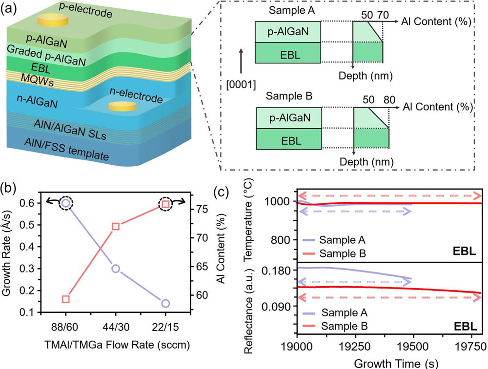
Figure 1: (a) DUV LED schematic structures with inset samples A and B variations. (b) Growth rate and Al content in AlGaN versus TMAl/TMGa flow rate. (c) In-situ temperature and reflectance transients during epitaxial growth of EBL and graded p-AlGaN.
The DUV LEDs (Figure 1) were grown using nitrogen-rich MOCVD on c-plane (0001) flat sapphire substrate (FSS). The precursors were trimethyl-Ga/Al (TM-Ga/Al) and ammonia (NH3). The n- and p-type dopants were silane (SiH4) and bis-cyclopentadienyl magnesium.
The LED structure included 3μm AlN template, 120nm Al0.7Ga0.3N transition, 70nm AlN/AlGaN superlattice (SL), 1μm n-AlGaN, multiple quantum well (MQW), 40nm EBL, 30nm graded p-AlGaN, and 20nm p-AlGaN layers. The five-period MQW consisted of 2nm Al0.4Ga0.6N wells separated by 10nm Al0.6Ga0.4N barriers.
The difference between the reference sample A and optimized sample B came in the EBL and graded p-AlGaN regions. The EBL differed in Al content: the 70% Al content of sample A was increased to 80%, and the gradings were changed respectively from 70–50 to 80–50%. In both cases, the 10nm p-contact layer had 40% Al. The EBL growth temperature was 1050°C. After the MOCVD growth, both samples were annealed at 750°C in nitrogen to activate the p-type doping.
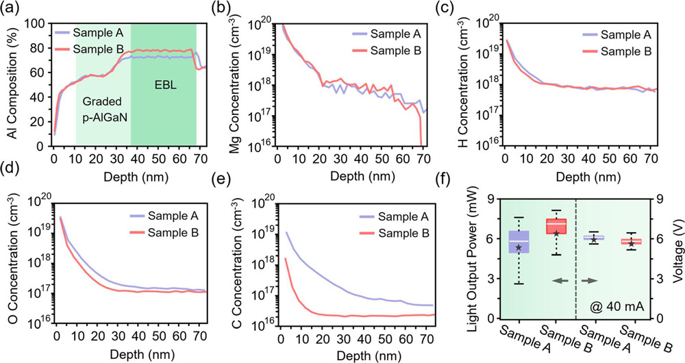
The researchers carefully studied the effects of varying the precursor flow rates to optimize Al incorporation in the high content layers. Naturally, the slower flow rates needed for higher Al content required longer processing times to achieve the same layer thickness. In particular, the slower growth of sample B enabled reduction in the C content to the order of 1016/cm3, almost an order of magnitude lower than for A.
The team suggests that the lower TMGa/Al flow rates enabled more of the carbon to be converted to methane (CH4), rather than incorporated into the AlGaN material, through reactions like:
N–H + Ga–CH3 → GaN + CH4
The researchers comment: “This reaction is facilitated by a higher partial pressure of NH3, which reduces carbon incorporation into the AlGaN layer. A reduced metal-organic precursor flow corresponds to a higher V/III ratio, which may explain the reduced carbon incorporation in the EBL of sample B.”
The researchers used the samples to fabricate 254μm x 508μm DUV LEDs with 450nm deep mesas produced using inductively coupled plasma (ICP) etch. The surfaces were passivated with plasma-enhanced CVD silicon dioxide.
One enhancement of using the optimized sample B was reduced contact resistance between the p-AlGaN and nickel/gold p-electrode: 2.8Ω-cm2, compared with 3.3Ω-cm2 for sample A. “This can be attributed to the increased hole concentration in p-regions, including the EBL and graded p-AlGaN layer,” the team explains.
The researchers speculate that the higher Al contents of sample B increases the C impurity ionization energy, while lower impurity concentrations also reduce point defect density, enhancing carrier transport. The hole concentration should also be increased by a higher induced polarization charge from the steeper grading in sample B.

Figure 2: Secondary-ion-mass spectroscopy (SIMS) results of (a) aluminium, (b) magnesium, (c) hydrogen, (d) oxygen, and (e) carbon. (f) Statistics for optoelectronic performance of DUV LED chips for each sample across 2-inch wafer. Black star, white horizontal line, and black vertical dotted line represent mean, median and 1.5x interquartile range of data, respectively.
The optimized sample B achieved higher average light output power and lower operating voltage 40mA injection, both of which factors contribute to higher efficiency (Figure 2). The averages were made over 10,000 chips from each sample material. The mean LOPs were 5.3mW and 6.4mW for A and B, respectively. The corresponding forward voltages were 5.9V and 5.6V.
https://doi.org/10.1063/5.0247937
The author Mike Cooke is a freelance technology journalist who has worked in the semiconductor and advanced technology sectors since 1997.


